DRV8334: Dead time much higher than expected

Part Number: DRV8334

Tool/software:

Dear technical team,

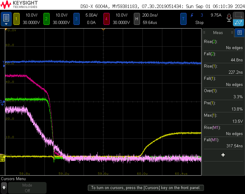
I'm optimizing the settings for my design and noticed the dead time is much higher than expected. I use DEADT_MODE = 1 (Dead time is inserted by monitoring gate driver outputs (GHx or GLx)) and DEADT = 001b (214 ns).

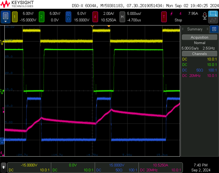
So GLx should start to increase the latest about 300ns after GHx reaches 0V. However I measure almost 800ns what is odd. The time increases / decreases when changing DEADT setting by about the right amount, but I have an offset of ca. 600ns.

The MOSFET used is BSC039N06NS.

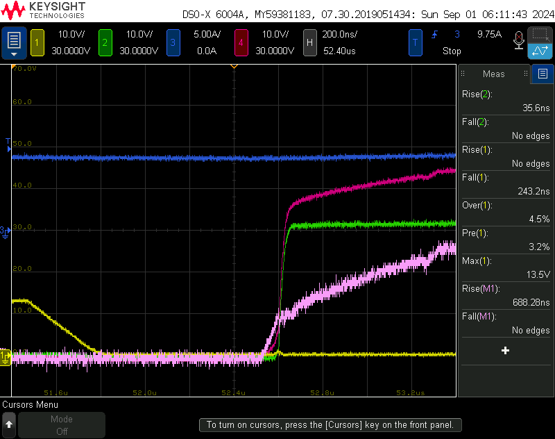
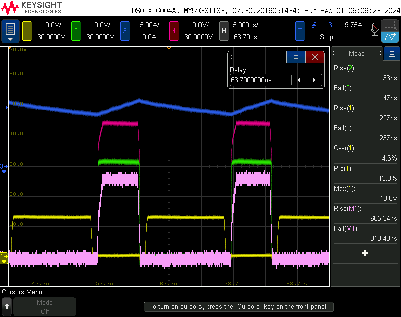
CH1 (Yellow): GLx

CH2 (Green): SWx

CH3 (Blue): Phase current

CH4 (Red): GHx

Math (Pink): GHx - SWx = high side FET Vgs
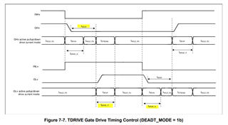
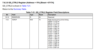
I use quite generous settings for TDRVP (750ns) and TDRVN (464ns). Does this interfere with the dead time? As I read the diagram it should not.

Please advise.


Thank you and kind regards
Stefan

  • Hi Stefan,

    Can you tell me a little more about your design? Like do you have any gate resistance or capacitance?

    Regards,

    Yara

  • Hello Yara,

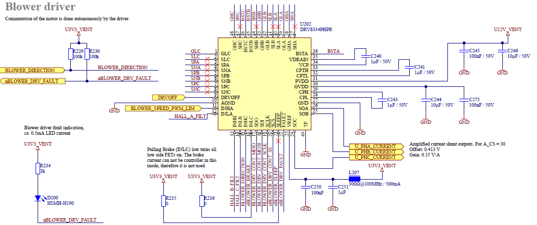
    sure I can show you the snippets of the schematic. I have to possibility to add gate resistance and capacitance, but so far they are not used. I do not have any snubber. The only special thing in my circuit is the output filter as the motor itself has a very low inductance (around 20uH).

    If you also need the settings for every singe register just let me know.

    Kind regards

    Stefan

  • Hi Stefan,

    Thanks for the schematic. At what point are you measuring GHx, SHx and GLx? Is it as close to the driver pins as possible? I'm not really sure what the issue could be other than the G-S resistor, maybe the value is too high? I'll consult my team to see if there are any additional possibilities.

    Regards,

    Yara

  • Hello Yara,

    the signals are measured at the FET. But I just measured again and at the driver and they are the same.

    I'm happy to test with a different G-S resistor value if you suggest one. However I don't think they are responsible for the effect.

    Best regards,

    Stefan

  • Hi Stefan,

    Have you tried adjusting your BSTx cap at all?
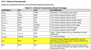
    While the BSTx capacitor itself doesn’t directly influence dead time, if the capacitor’s value is too low, it could lead to slow charging of the high-side gate drive, causing delays in high-side MOSFET activation. This might explain part of the offset if the capacitor is not properly sized.

    Did you use the following guidelines when selecting the BSTx capacitor?

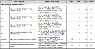
    The DRV8334 has built-in propagation delays between the input signal and the switching action on the MOSFETs. These delays can vary depending on the gate driver’s design and can introduce an offset that might be what you’re observing. However the max propagation delay listed is 150ns, significantly less than the 600ns offset you're seeing.

    Do your input signals align with the expected timing?

    Regards,

    Yara

  • Hello Yara,

    from my original notes on BST capacitor:

    The capacitor I use has 280nF @ 12V what should be plenty even under worst case condition. For testing I doubled the capacitance, but there is no change in the dead time.

    I can see the gate starts switching about 150ns after the INHA pin changes (1x PWM mode). This is expected, but the dead time is still very high.

    Regards,

    Stefan

  • Hello Yara,

    I found an error in my schematic, the pin 35 (VDRAIN) was not connected to U_BLOWER. As a result the charge pump was not working. I fixed the error, but sadly no change on the dead time despite VGS is constantly about 10V above U_BLOWER.

    Regards,

    Stefan

  • Hi Stefan,

    Can I get a waveform of your input signals and output signals so I can bring this issue to my team?

    Regards,

    Yara

  • Hi Yara,

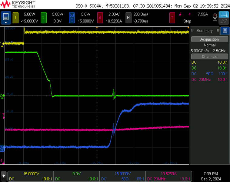
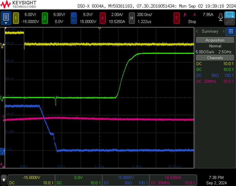
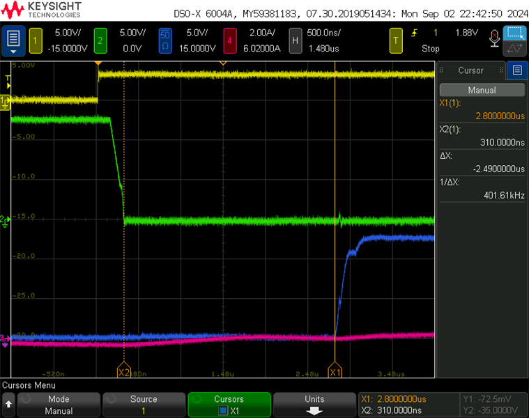
    I'm sorry for the late reply but I got sick and wasn't in the office for a few days. Here are the measurements, all signals were measured directly at the DRV8334.

    CH1: PWM input on INHA (1x PWM mode)
    CH2: GLC, low side FET gate voltage
    CH3: GHC - SHC, high side FET gate voltage (measured with high bandwidth differential probe)
    CH4: Motor current phase C

    The gate current is set quite aggressive to increase the switching speed and reduce their influence on the dead time. Once the dead time is solved I will slow them down again as this causes significant cross talk on the gates when the node SWC slews.

    If you need more measurements just let me know.

    Best regards

    Stefan

  • Hi Stefan, 

    I think I may understand what is happening now.

    The time between GHx going low and GLx going high isn't all dead time, part of this time is also TDRIVE

    What is your TDRVP and TDRNP settings in the following register?

    You could try adjusting this and see if the affects the 600ns offset you've been seeing?

    Regards,

    Yara

  • Hi Yara,

    the settings for the measurements were:
    DEADT = 0b000U; // 70ns
    TDRVP = 0b0001U; // 179ns
    TDRVN_D = 0b0000U; // 70ns
    TDRVN = 0b0001U; // 179ns

    I don't think the TDRVP / TDRVN time has an influence. I just tested with TDRVP / TDRVN = 1600ns, but the dead time is still 600ns.

    Kind regards,

    Stefan

  • Hi Stefan,

    I just tested with TDRVP / TDRVN = 1600ns, but the dead time is still 600ns

    did you mean the deadtime offset is still 600ns?

    I'll have to re-group with my team I'll give an update by EOD tomorrow.

    Regards,

    Yara

  • Hi Yara,

    no I mean the waveform is exactly the same regardless of TDRVP / TDRVN.

    Regards,

    Stefan

  • Hi Stefan,

    I think what you may being seeing is expected behavior and could be a combination of the variation in the deadtime:

    as well as propagation delay

    the way deadtime is measure with this device is a little different than our other devices, and when deadtime starts and finishes can change based on the settings selected.

    Have you tried using DEADT_MODE = 0?

    Regards,

    Yara

  • Hi Yara,

    I don't really agree that this is expected behavior.

    1) Dead time
    I measure the dead time from GLC reaching 0V to high side FET gate start rising. The max tolerance for DEADTIME = 000 is 130ns, while I measure 600ns. This is not expected, even if we add 150ns propagation delay (what is wrong in my opinion as is it measured from the input to the first FET gate voltage change).

    2) Propagation delay
    GLC starts falling about 150ns after the PWM input rises. This is in line with the propagation delay and expected. But please note the propagation delay is not included in the dead time I measure.

    I tried using DEADT_MODE = 0 and 1 as well as SGD_MODE = 0 and 1. While I see the changes, the dead time is always about 600ns longer than expected.

    I mean the dead time lowers the efficiency what is somewhat acceptable. I'm more worried that I don't understand whats going on and the offset may disappear for some reason in the future, pushing us extremely close to cross conduction risks given we have the lowest setting in most timing registers.

    Regards,

    Stefan

  • Hi Stefan,

    I'm meeting with my team tomorrow, I will bring up this issue as it has me a little stumped. Thank you for all the information you've given so far!

    Regards,

    Yara

  • Hi Stefan,

    So I met with my team and we have some suggestions as well as some more questions:

    The most recent waveforms that were sent, what was the deadtime selected? Because it looks to be pretty close to 600ns? Do you have waveforms of the highest de4adtime setting?

    Is this behavior seen on multiple units?

    Something that was suggested was to try 3x PWM and see if your are observing the same behavior.

    I'll be trying to get my hands on an EVM to see if I can test it in lab.

    Regards,

    Yara

  • Hi Yara,

    sure let me answer your questions:

    1) Dead time setting:
    This was already answered in my previous post:

    DEADT = 0b000U; // 70ns
    TDRVP = 0b0001U; // 179ns
    TDRVN_D = 0b0000U; // 70ns
    TDRVN = 0b0001U; // 179ns

    With the highest dead time setting (2000ns) I measure 2490ns:

    2) Different units:
    I tested again with a different unit this morning, same behavior.

    3) PWM Mode:
    I use the 1x PWM and a motor with Hall sensors and the DRV8334 handles the commutation. Changing it to 3x PWM would not only require a complete redesign on the board, but also additional software development. This is simply not possible and even if it would solve the dead time issue, we will not switch to 3x PWM mode. In fact the 1x PWM mode was the main reason for selecting the DRV8334 over other drivers.

    Please go ahead an measure with the EVM, I'm slowly but surely running out of time to solve the issue.

    Kind regards

    Stefan

  • Hi Stefan,

    I'm still working to get in lab and test this out myself.

    In the mean time I think I may need to clarify that I'm not recommending you change your design or switch to 3x PWM rather just test in 3x PWM by changing the setting via SPI, tying INLx high, and using a function generator for INHx. Then you can observe the outputs?

    Regards,

    Yara

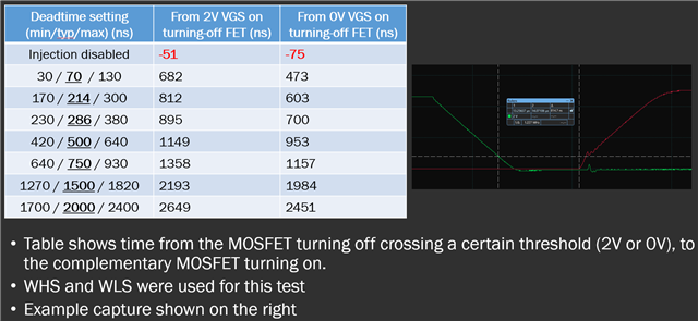
  • Hello, chiming in on this request as I've done some testing of deadtime and am seeing the same anomaly--but only when doing output-based deadtime injection (which is what I want to do so I can keep the deadtime as low as possible / let the gate driver's output monitoring take MOSFET, IDrive, etc. tolerancing out of the equation). Here are the results from my testing of various output-based deadtime injection settings when using some FW that would switch between HS and LS FETs on the same phase rapidly.

  • Hello Jonathan,

    thanks for the additional input, good to know I'm not the only one. What PWM mode do you use (1x/3x/6x)?

    Regards, Stefan

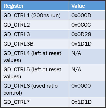
  • Hi Stefan, I'm doing 6x. Here's my full register settings at present for reference.

  • Hello Jonathan,

    Thank you for adding in your findings! I'm bringing this to our systems engineers to see if they have any comments.

    Regards,

    Yara

  • Hi all,

    I talked with some of my contacts at TI earlier today about this and have an explanation. As you can see in the able above, the times were consistent but all had about ~400-600ns added to them (really depends on how you want to measure it--ideally from the lowest VGS monitor threshold voltage for "off" MOSFET to the complementary MOSFET starting to turn on).

    This is because of the analog comparator architecture of the DRV8334, largely--it needs to not just detect VGS being within the spec, but compensate for noise also through deglitch timing (think about how much the high-side MOSFET source can shift during operation. Hard to design silicon for that to monitor VGS perfectly at a very high bandwidth). I am told that this is more or less how it is in all other gate drivers also--though the 8334's architecture should be improved slightly with regards to response time.

    In reality, it seems that the deadtime injection system is working perfectly--it's just a datasheet spec that doesn't tell the whole story. Hope this helps--let me know if I can help clarify on anything.

  • Hi Jonathan,

    Thank you for the clarification! I'll add on to the thread if I get any additional information.

    Regards,

    Yara

  • Hi Jonathan,

    oh you have a really experienced contact at TI, one could get jealous :)

    The technical explanation is reasonable, but this fact is really poorly noted in the datasheet. As I use the 1x PWM mode the deadtime is always inserted regardless of DEADT_MODE setting, so I just have to live with it. At least I'm not concerned now setting the deadtime to the lowest value.

    @Yara, please consider updating the datasheet and thanks for your support.

    Regards

    Stefan