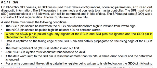
Tool/software:
Hi dear community,
I hope you are all doing well.
I am using an STM32G431KBT6 development board, and I need to configure the registers of a DRV8323RS motor driver. For this project, I connected the SPI pins correctly using the BOOSTXL-DRV8323RS development board and set the SPI clock to 1 MHz. I’m working in the Arduino IDE.
Specifically, I am trying to configure the following registers:
- 0x02 (Control Register): 0x1201
- 0x03 (Gate Drive HS Register): 0x1BFF
- 0x04 (Gate Drive LS Register): 0x27FF
- 0x05 (OCP Control Register): 0x295F
- 0x06 (CSA Control Register): 0x3083
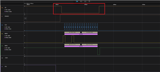
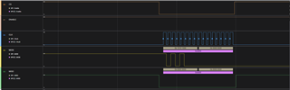
Using a logic analyzer, I can confirm that the SPI clock, CS pin, and transmitted data (MOSI) from the STM32G431KBT6 are correct. The enable pin is also functioning properly. However, the data returned from the DRV8323RS is not as expected.
I ensured that the communication follows the format described in the datasheet under the "Programming" section (Page 52/111). I expected to read back the values I wrote to the registers, but I’m receiving unexpected data that I don't understand.
Even when I ignored the returned data and tried changing the 1PWM_DIR bit in the Control Register to reverse the motor’s direction, there was no effect. It seems the registers are not being written correctly, even though the transmitted bytes appear valid.
I’ve double-checked the hardware connections for any interference and used an oscilloscope to analyze the analog signals, which match the logic analyzer results. I also confirmed that the SPI configurations between the master and slave are consistent, including MSBFIRST, SPI mode, and timing requirements.
Can you help me identify the cause of this issue? What changes or corrections can I make to read back the correct register values and ensure the settings are properly applied?
I will share the Arduino IDE code, logic analyzer screenshots, and hardware setup details for further insights.
The reason I am working on this is to control a BLDC motor with 393KV, 20 poles, and 10 pole pairs using FOC (Field-Oriented Control) with the SimpleFOC library. However, I’ve encountered problems with current consumption and motor heating. I suspect these issues could be related to incorrect driver configurations, particularly with the TDRIVE, IDRIVEP_LS, IDRIVEN_LS settings in the Gate Drive LS Register, and IDRIVEP_HS, IDRIVEN_HS settings in the Gate Drive HS Register, which control peak source and sink gate currents.
Any guidance or suggestions would be greatly appreciated!


0x02 Write Read


0x03 Write Read


0x04 Write Read


0x05 Write Read

0x06 Write Read


#include <SimpleFOC.h>
#include <SPI.h>
#include <stm32g4xx_hal.h>
#define ADR_DRV_CTRL 0x02
#define GATE_DRIVER_HS 0x03
#define GATE_DRIVER_LS 0x04
#define OCP_CONTROL 0x05
#define CSA_CONTROL 0x06
#define ADR_FAULT_STAT 0x00
#define SS_PIN PA4 // Define the SS (CS) pin
#define SCK_PIN PA5 // Define the SCK pin
#define MOSI_PIN PA7 // Define the MOSI pin
#define MISO_PIN PA6 // Define the MISO pin
#define _MON_TARGET 0b1000000 // monitor target value
#define _MON_VOLT_Q 0b0100000 // monitor voltage q value
#define _MON_VOLT_D 0b0010000 // monitor voltage d value
#define _MON_CURR_Q 0b0001000 // monitor current q value - if measured
#define _MON_CURR_D 0b0000100 // monitor current d value - if measured
#define _MON_VEL 0b0000010 // monitor velocity value
#define _MON_ANGLE 0b0000001 // monitor angle value
const int CS_PIN = PA4;
ADC_HandleTypeDef hadc1;
ADC_HandleTypeDef hadc2;
I2C_HandleTypeDef hi2c1;
SPI_HandleTypeDef hspi1;
TIM_HandleTypeDef htim1;
TIM_HandleTypeDef htim2;
TIM_HandleTypeDef htim3;
UART_HandleTypeDef huart2;
#define BUFFER_SIZE 100
uint8_t rxBuffer[BUFFER_SIZE]; // Buffer to store received data
uint8_t rxIndex = 0; // Index for the buffer
uint32_t adcValue = 0;
int adcValue1 = 0 ;
//-----------------------------------------------------------------END SPI PART
//stm32 defines
/* Private defines -----------------------------------------------------------*/
#define ADC_NTCMotorTemp_Pin GPIO_PIN_0
#define ADC_NTCMotorTemp_GPIO_Port GPIOF
#define ADC_Voltage_Pin GPIO_PIN_1
#define ADC_Voltage_GPIO_Port GPIOF
#define NRST_Pin GPIO_PIN_10
#define NRST_GPIO_Port GPIOG
#define INHC_Pin GPIO_PIN_0
#define INHC_GPIO_Port GPIOA
#define ADC_Pressure_Pin GPIO_PIN_1
#define ADC_Pressure_GPIO_Port GPIOA
#define UART_TX_NRF52_Pin GPIO_PIN_2
#define UART_TX_NRF52_GPIO_Port GPIOA
#define UART_RX_NRF52_Pin GPIO_PIN_3
#define UART_RX_NRF52_GPIO_Port GPIOA
#define ADC_BoardTemp_Pin GPIO_PIN_0
#define ADC_BoardTemp_GPIO_Port GPIOB
#define INHA_Pin GPIO_PIN_8
#define INHA_GPIO_Port GPIOA
#define INLA_Pin GPIO_PIN_9
#define INLA_GPIO_Port GPIOA
#define HALLB_Pin GPIO_PIN_10
#define HALLB_GPIO_Port GPIOA
#define HALLA_Pin GPIO_PIN_11
#define HALLA_GPIO_Port GPIOA
#define HALLC_Pin GPIO_PIN_12
#define HALLC_GPIO_Port GPIOA
#define INLC_Pin GPIO_PIN_3
#define INLC_GPIO_Port GPIOB
#define INHB_Pin GPIO_PIN_4
#define INHB_GPIO_Port GPIOB
#define INLB_Pin GPIO_PIN_5
#define INLB_GPIO_Port GPIOB
#define ENABLE_Pin GPIO_PIN_6
#define ENABLE_GPIO_Port GPIOB
#define BOOT0_Pin GPIO_PIN_8
#define BOOT0_GPIO_Port GPIOB
#define HALLA PA11
#define HALLB PA10
#define HALLC PA12 //PA11 //NEW PB11
#define INHA PA8 //TIM2 CH3 PA2 -----//new- //TIM1 CH1 PA8 //pb6
#define INHB PB4 //TIM4 CH1 PB6 //TIM1 CH4 PA11 ----- //new- //TIM1 CH2 PA9
#define INLA PA9 //TIM2 CH4 PA3 //new- //TIM1 CH1N PA7 //PB7
#define INLB PB5 //TIM4 CH2 PB7//TIM1 CH2 PA9 -----//new- //TIM1 CH2N PB0
#define INHC PA0 //TIM4 CH2 PB7//TIM1 CH2 PA9 -----//new- //TIM1 CH2N PB0
#define INLC PB3 //TIM4 CH4 PB9 //TIM1 CH1 PA8 ---- //new- //TIM1 CH3N PB1
#define ENABLEIO PB6
//-------------------------------------------------------------------------------------------------------------SPI PART
uint8_t m_tx_buf[2];
uint8_t m_rx_buf[2];
uint16_t tes_buf ;
uint16_t uint16_DRV8323_cfg;
#define PIN_ENABLE_DRV83 PB6
SPIClass etx_spi( PIN_SPI_MOSI, PIN_SPI_MISO, PIN_SPI_SCK );
SPISettings spiSettings(1000000, MSBFIRST, SPI_MODE0);
//-----------------------------------------------------------------BEGIN SPI PART
#define PIN_CAL_DRV83 PA1
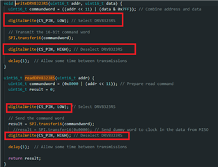
void writeDRV8323RS(uint16_t addr, uint16_t data) {
uint16_t commandword = ((addr << 11) | (data & 0x7FF)); // Combine address and data
//SPI.beginTransaction(SPISettings(1000000, MSBFIRST, SPI_MODE0)); // Set SPI speed to 1 MHz
digitalWrite(CS_PIN, LOW); // Select DRV8323RS
// Transmit the 16-bit command word
SPI.transfer16(commandword);
digitalWrite(CS_PIN, HIGH); // Deselect DRV8323RS
//SPI.endTransaction();
delay(1); // Allow some time between transmissions
}
uint16_t readDRV8323RS(uint16_t addr) {
uint16_t commandword = (0x8000 | (addr << 11)); // Prepare read command
uint16_t result = 0;
digitalWrite(CS_PIN, LOW); // Select DRV8323RS
result = SPI.transfer16(commandword);
digitalWrite(CS_PIN, HIGH);
delay(1);
return result;
}
void configureDRV8323RS() {
// Example: Configure the Control Register 1 (address 0x02) of DRV8323RS
uint16_t address0x02 = 0x02; // Address of Control Register 1
uint16_t data0x02 = 0x1201; // Example data to configure the register (replace with actual values)
uint16_t address0x03 = 0x03; // Address of Control Register 1
uint16_t data0x03 = 0x1BFF; // Example data to configure the register (replace with actual values)
uint16_t address0x04 = 0x04; // Address of Control Register 1
uint16_t data0x04 = 0x27FF; // Example data to configure the register (replace with actual values)
uint16_t address0x05 = 0x05; // Address of Control Register 1
uint16_t data0x05 = 0x295F; // Example data to configure the register (replace with actual values)
uint16_t address0x06 = 0x06; // Address of Control Register 1
uint16_t data0x06 = 0x3083; // Example data to configure the register (replace with actual values)
Serial.print("Writing to DRV8323RS Register 0x");
Serial.print(address0x02, HEX);
Serial.print(": 0x");
Serial.println(data0x02, HEX);
Serial.print("Writing to DRV8323RS Register 0x");
Serial.print(address0x03, HEX);
Serial.print(": 0x");
Serial.println(data0x03, HEX);
Serial.print("Writing to DRV8323RS Register 0x");
Serial.print(address0x04, HEX);
Serial.print(": 0x");
Serial.println(data0x04, HEX);
Serial.print("Writing to DRV8323RS Register 0x");
Serial.print(address0x05, HEX);
Serial.print(": 0x");
Serial.println(data0x05, HEX);
Serial.print("Writing to DRV8323RS Register 0x");
Serial.print(address0x06, HEX);
Serial.print(": 0x");
Serial.println(data0x06, HEX);
// Write to the register
pinMode(PIN_ENABLE_DRV83, OUTPUT);
pinMode(PIN_CAL_DRV83, OUTPUT);
digitalWrite(PIN_ENABLE_DRV83, LOW);
//digitalWrite(PIN_BRAKE_DRV83, HIGH);
digitalWrite(PIN_CAL_DRV83, LOW);
digitalWrite(PIN_ENABLE_DRV83, HIGH);
timer_delay_ms(2);
digitalWrite(PIN_ENABLE_DRV83, LOW);
timer_delay_ms(2);
digitalWrite(PIN_ENABLE_DRV83, HIGH);
timer_delay_ms(10);
writeDRV8323RS(address0x02, data0x02);
timer_delay_ms(10);
uint16_t readData = readDRV8323RS(address0x02);
Serial.print("Read back data: 0x");
Serial.println(readData, HEX);
digitalWrite(PIN_ENABLE_DRV83, LOW);
//digitalWrite(PIN_BRAKE_DRV83, HIGH);
digitalWrite(PIN_CAL_DRV83, LOW);
digitalWrite(PIN_ENABLE_DRV83, HIGH);
timer_delay_ms(2);
digitalWrite(PIN_ENABLE_DRV83, LOW);
timer_delay_ms(2);
digitalWrite(PIN_ENABLE_DRV83, HIGH);
timer_delay_ms(10);
writeDRV8323RS(address0x03, data0x03);
timer_delay_ms(10);
readData = readDRV8323RS(address0x03);
Serial.print("Read back data: 0x");
Serial.println(readData, HEX);
digitalWrite(PIN_ENABLE_DRV83, LOW);
//digitalWrite(PIN_BRAKE_DRV83, HIGH);
digitalWrite(PIN_CAL_DRV83, LOW);
digitalWrite(PIN_ENABLE_DRV83, HIGH);
timer_delay_ms(2);
digitalWrite(PIN_ENABLE_DRV83, LOW);
timer_delay_ms(2);
digitalWrite(PIN_ENABLE_DRV83, HIGH);
timer_delay_ms(10);
writeDRV8323RS(address0x04, data0x04);
timer_delay_ms(10);
readData = readDRV8323RS(address0x04);
Serial.print("Read back data: 0x");
Serial.println(readData, HEX);
digitalWrite(PIN_ENABLE_DRV83, LOW);
//digitalWrite(PIN_BRAKE_DRV83, HIGH);
digitalWrite(PIN_CAL_DRV83, LOW);
digitalWrite(PIN_ENABLE_DRV83, HIGH);
timer_delay_ms(2);
digitalWrite(PIN_ENABLE_DRV83, LOW);
timer_delay_ms(2);
digitalWrite(PIN_ENABLE_DRV83, HIGH);
timer_delay_ms(10);
writeDRV8323RS(address0x05, data0x05);
timer_delay_ms(10);
readData = readDRV8323RS(address0x05);
Serial.print("Read back data: 0x");
Serial.println(readData, HEX);
digitalWrite(PIN_ENABLE_DRV83, LOW);
//digitalWrite(PIN_BRAKE_DRV83, HIGH);
digitalWrite(PIN_CAL_DRV83, LOW);
digitalWrite(PIN_ENABLE_DRV83, HIGH);
timer_delay_ms(2);
digitalWrite(PIN_ENABLE_DRV83, LOW);
timer_delay_ms(2);
digitalWrite(PIN_ENABLE_DRV83, HIGH);
timer_delay_ms(10);
writeDRV8323RS(address0x06, data0x06);
timer_delay_ms(10);
readData = readDRV8323RS(address0x06);
// Read back the register to verify
Serial.print("Read back data: 0x");
Serial.println(readData, HEX);
timer_delay_ms(2);
timer_delay_ms(2);
digitalWrite(PIN_CAL_DRV83, HIGH);
timer_delay_ms(2);
digitalWrite(PIN_CAL_DRV83, LOW);
timer_delay_ms(2);
// Repeat for other registers as needed
}
void timer_delay_ms(uint16_t ms) {
delay(ms);
}
//-------------------------------------------------------------------------------------------------------------SPI PART
float rpm = 0;
float rpm_pot = 0;
float needReinitialize = 0;
float zero_electrical_angle_eeprom = 0;
float sensor_direction_eeprom = 0;
unsigned long previousMillis = 0; // Store last time RPM was updated
const long interval = 2000; // Interval at which to update RPM (milliseconds) //250
HallSensor sensor = HallSensor(HALLA, HALLB, HALLC, 10);// U V W Pole Pairs
void doA(){sensor.handleA();}
void doB(){sensor.handleB();}
void doC(){sensor.handleC();}
//Motor parameters: Set the number of pole pairs according to the motor
BLDCMotor motor = BLDCMotor(10);
BLDCDriver6PWM driver = BLDCDriver6PWM(INHA,INLA,INHB,INLB,INHC,INLC,ENABLEIO);
bool flag_run = false;
float target_velocity = (rpm * (2.0 * PI))/(60.0);
Commander command = Commander(Serial);
void doTarget(char* cmd) { command.scalar(&rpm, cmd); }
void doTarget2(char* cmd) { command.scalar(&needReinitialize, cmd); }
void calcKV() {
// calculate the KV
float rpm1 = (motor.shaft_velocity* 60.0 )/(2.0 * PI);
float Target_rpm = (target_velocity* 60.0 )/(2.0 * PI);
Serial.print(rpm1); //the first variable for plotting
Serial.print(","); //seperator
Serial.println(rpm);
}
void Potentiometre_RPM_FRB(){
adcValue1 = analogRead(PB0);
//Serial.println(adcValue1);
if (adcValue1 < 200 && rpm_pot != 0){
rpm_pot = 0 ;
rpm = rpm_pot ;
Serial.println(adcValue1);
Serial.println("rpm = 0 ");
}
if (adcValue1 > 400 && adcValue1 < 700 && rpm_pot != 500){
rpm_pot = 500 ;
rpm = rpm_pot ;
Serial.println(adcValue1);
Serial.println("rpm = 500 ");
}
if (adcValue1 > 900 && adcValue1 < 1500 && rpm_pot != 1000){
rpm_pot = 1000 ;
rpm = rpm_pot ;
Serial.println(adcValue1);
Serial.println("rpm = 1000");
}
if (adcValue1 > 1700 && adcValue1 < 2040 && rpm_pot != 1500 ) {
rpm_pot = 1500 ;
rpm = rpm_pot ;
Serial.println(adcValue1);
Serial.println("rpm = 1500 ");
}
if ( adcValue1 > 2300 && adcValue1 < 2720 && rpm_pot != 2000 ) {
rpm_pot = 2000 ;
rpm = rpm_pot ;
Serial.println(adcValue1);
Serial.println("rpm = 2000 ");
}
if (adcValue1 > 3000 && adcValue1 < 3400 && rpm_pot != 2500 ) {
rpm_pot = 2500 ;
rpm = rpm_pot ;
Serial.println(adcValue1);
Serial.println("rpm = 2500 ");
}
if ( adcValue1 > 3600 && rpm_pot != 3000) {
rpm_pot = 3000 ;
rpm = rpm_pot ;
Serial.println(adcValue1);
Serial.println("rpm = 3000 ");
}
}
void Potentiometre_RPM_FIS(){
adcValue1 = analogRead(PB0);
//Serial.println(adcValue1);
if (adcValue1 < 200 && rpm_pot != 0){
rpm_pot = 0 ;
rpm = rpm_pot ;
Serial.println(adcValue1);
Serial.println("rpm = 0 ");
}
if (adcValue1 > 400 && adcValue1 < 700 && rpm_pot != 4000){
rpm_pot = 4000 ;
rpm = rpm_pot ;
Serial.println(adcValue1);
Serial.println("rpm = 4000 ");
}
if (adcValue1 > 900 && adcValue1 < 1500 && rpm_pot != 5000){
rpm_pot = 5000 ;
rpm = rpm_pot ;
Serial.println(adcValue1);
Serial.println("rpm = 5000");
}
if (adcValue1 > 1700 && adcValue1 < 2040 && rpm_pot != 6000 ) {
rpm_pot = 6000 ;
rpm = rpm_pot ;
Serial.println(adcValue1);
Serial.println("rpm = 6000 ");
}
if ( adcValue1 > 2300 && adcValue1 < 2720 && rpm_pot != 7000 ) {
rpm_pot = 7000 ;
rpm = rpm_pot ;
Serial.println(adcValue1);
Serial.println("rpm = 7000 ");
}
if (adcValue1 > 3000 && adcValue1 < 3400 && rpm_pot != 8000 ) {
rpm_pot = 8000 ;
rpm = rpm_pot ;
Serial.println(adcValue1);
Serial.println("rpm = 8000 ");
}
if ( adcValue1 > 3600 && rpm_pot != 8000) {
rpm_pot = 8000 ;
rpm = rpm_pot ;
Serial.println(adcValue1);
Serial.println("rpm = 8000 ");
}
}
void Potentiometre_RPM_FOB(){
adcValue1 = analogRead(PB0);
//Serial.println(adcValue1);
if (adcValue1 < 200 && rpm_pot != 0){
rpm_pot = 0 ;
rpm = rpm_pot ;
Serial.println(adcValue1);
Serial.println("rpm = 0 ");
}
if (adcValue1 > 400 && adcValue1 < 700 && rpm_pot != 3000){
rpm_pot = 3000 ;
rpm = rpm_pot ;
Serial.println(adcValue1);
Serial.println("rpm = 3000 ");
}
if (adcValue1 > 900 && adcValue1 < 1500 && rpm_pot != 4000){
rpm_pot = 4000 ;
rpm = rpm_pot ;
Serial.println(adcValue1);
Serial.println("rpm = 4000");
}
if (adcValue1 > 1700 && adcValue1 < 2040 && rpm_pot != 5000 ) {
rpm_pot = 5000 ;
rpm = rpm_pot ;
Serial.println(adcValue1);
Serial.println("rpm = 5000 ");
}
if ( adcValue1 > 2300 && adcValue1 < 2720 && rpm_pot != 6000 ) {
rpm_pot = 6000 ;
rpm = rpm_pot ;
Serial.println(adcValue1);
Serial.println("rpm = 6000 ");
}
if (adcValue1 > 3000 && adcValue1 < 3400 && rpm_pot != 7000 ) {
rpm_pot = 7000 ;
rpm = rpm_pot ;
Serial.println(adcValue1);
Serial.println("rpm = 7000 ");
}
if ( adcValue1 > 3600 && rpm_pot != 8000) {
rpm_pot = 8000 ;
rpm = rpm_pot ;
Serial.println(adcValue1);
Serial.println("rpm = 8000 ");
}
}
void SystemClock_Config(void)
{
RCC_OscInitTypeDef RCC_OscInitStruct = {0};
RCC_ClkInitTypeDef RCC_ClkInitStruct = {0};
/** Configure the main internal regulator output voltage
*/
HAL_PWREx_ControlVoltageScaling(PWR_REGULATOR_VOLTAGE_SCALE1_BOOST);
/** Initializes the RCC Oscillators according to the specified parameters
* in the RCC_OscInitTypeDef structure.
*/
RCC_OscInitStruct.OscillatorType = RCC_OSCILLATORTYPE_HSI;
RCC_OscInitStruct.HSIState = RCC_HSI_ON;
RCC_OscInitStruct.HSICalibrationValue = RCC_HSICALIBRATION_DEFAULT;
RCC_OscInitStruct.PLL.PLLState = RCC_PLL_ON;
RCC_OscInitStruct.PLL.PLLSource = RCC_PLLSOURCE_HSI;
RCC_OscInitStruct.PLL.PLLM = RCC_PLLM_DIV4;
RCC_OscInitStruct.PLL.PLLN = 85;
RCC_OscInitStruct.PLL.PLLP = RCC_PLLP_DIV2;
RCC_OscInitStruct.PLL.PLLQ = RCC_PLLQ_DIV2;
RCC_OscInitStruct.PLL.PLLR = RCC_PLLR_DIV2;
if (HAL_RCC_OscConfig(&RCC_OscInitStruct) != HAL_OK)
{
Error_Handler();
}
/** Initializes the CPU, AHB and APB buses clocks
*/
RCC_ClkInitStruct.ClockType = RCC_CLOCKTYPE_HCLK|RCC_CLOCKTYPE_SYSCLK
|RCC_CLOCKTYPE_PCLK1|RCC_CLOCKTYPE_PCLK2;
RCC_ClkInitStruct.SYSCLKSource = RCC_SYSCLKSOURCE_PLLCLK;
RCC_ClkInitStruct.AHBCLKDivider = RCC_SYSCLK_DIV1;
RCC_ClkInitStruct.APB1CLKDivider = RCC_HCLK_DIV1;
RCC_ClkInitStruct.APB2CLKDivider = RCC_HCLK_DIV1;
if (HAL_RCC_ClockConfig(&RCC_ClkInitStruct, FLASH_LATENCY_4) != HAL_OK)
{
Error_Handler();
}
}
void Errors_Handler(void)
{
// User can add their own implementation to report the HAL error return state
while(1)
{
}
}
void printPWMConfig(TIM_HandleTypeDef* htim) {
// Get the Timer's Prescaler and ARR
uint32_t prescaler = htim->Init.Prescaler;
uint32_t arr = htim->Init.Period;
// Get the system clock configuration
RCC_ClkInitTypeDef clk_init;
uint32_t flash_latency;
HAL_RCC_GetClockConfig(&clk_init, &flash_latency);
// Calculate APB1 Timer Clock Frequency
uint32_t apb1_freq = HAL_RCC_GetPCLK1Freq();
uint32_t apb1_timer_freq;
if (clk_init.APB1CLKDivider == RCC_HCLK_DIV1) {
apb1_timer_freq = apb1_freq;
} else {
apb1_timer_freq = apb1_freq * 2;
}
// Calculate the Timer Clock Frequency considering the prescaler
uint32_t timerClockFreq = apb1_timer_freq / (prescaler + 1);
// Calculate PWM Frequency
uint32_t pwmFrequency = timerClockFreq / (arr + 1);
// Print the values
Serial.print("Prescaler: ");
Serial.println(prescaler);
Serial.print("ARR: ");
Serial.println(arr);
Serial.print("CPU Frequency HCLK: ");
Serial.print(HAL_RCC_GetHCLKFreq());
Serial.println(" Hz");
Serial.print("CPU Frequency SYSCLK: ");
Serial.print(HAL_RCC_GetSysClockFreq());
Serial.println(" Hz");
Serial.print("APB1 Peripheral Clock Frequency: ");
Serial.print(apb1_freq);
Serial.println(" Hz");
Serial.print("APB1 Timer Clock Frequency: ");
Serial.print(apb1_timer_freq);
Serial.println(" Hz");
Serial.print("Timer Clock Frequency: ");
Serial.print(timerClockFreq);
Serial.println(" Hz");
Serial.print("PWM Frequency: ");
Serial.print(pwmFrequency);
Serial.println(" Hz");
}
void HAL_TIM_MspPostInit(TIM_HandleTypeDef* htim)
{
GPIO_InitTypeDef GPIO_InitStruct = {0};
if(htim->Instance==TIM1)
{
/* USER CODE BEGIN TIM1_MspPostInit 0 */
/* USER CODE END TIM1_MspPostInit 0 */
__HAL_RCC_GPIOA_CLK_ENABLE();
/**TIM1 GPIO Configuration
PA8 ------> TIM1_CH1
PA9 ------> TIM1_CH2
*/
GPIO_InitStruct.Pin = INHA_Pin|INLA_Pin;
GPIO_InitStruct.Mode = GPIO_MODE_AF_PP;
GPIO_InitStruct.Pull = GPIO_NOPULL;
GPIO_InitStruct.Speed = GPIO_SPEED_FREQ_LOW;
GPIO_InitStruct.Alternate = GPIO_AF6_TIM1;
HAL_GPIO_Init(GPIOA, &GPIO_InitStruct);
/* USER CODE BEGIN TIM1_MspPostInit 1 */
/* USER CODE END TIM1_MspPostInit 1 */
}
else if(htim->Instance==TIM2)
{
/* USER CODE BEGIN TIM2_MspPostInit 0 */
/* USER CODE END TIM2_MspPostInit 0 */
__HAL_RCC_GPIOA_CLK_ENABLE();
__HAL_RCC_GPIOB_CLK_ENABLE();
/**TIM2 GPIO Configuration
PA0 ------> TIM2_CH1
PB3 ------> TIM2_CH2
*/
GPIO_InitStruct.Pin = INHC_Pin;
GPIO_InitStruct.Mode = GPIO_MODE_AF_PP;
GPIO_InitStruct.Pull = GPIO_NOPULL;
GPIO_InitStruct.Speed = GPIO_SPEED_FREQ_LOW;
GPIO_InitStruct.Alternate = GPIO_AF1_TIM2;
HAL_GPIO_Init(INHC_GPIO_Port, &GPIO_InitStruct);
GPIO_InitStruct.Pin = INLC_Pin;
GPIO_InitStruct.Mode = GPIO_MODE_AF_PP;
GPIO_InitStruct.Pull = GPIO_NOPULL;
GPIO_InitStruct.Speed = GPIO_SPEED_FREQ_LOW;
GPIO_InitStruct.Alternate = GPIO_AF1_TIM2;
HAL_GPIO_Init(INLC_GPIO_Port, &GPIO_InitStruct);
/* USER CODE BEGIN TIM2_MspPostInit 1 */
/* USER CODE END TIM2_MspPostInit 1 */
}
else if(htim->Instance==TIM3)
{
/* USER CODE BEGIN TIM3_MspPostInit 0 */
/* USER CODE END TIM3_MspPostInit 0 */
__HAL_RCC_GPIOB_CLK_ENABLE();
/**TIM3 GPIO Configuration
PB4 ------> TIM3_CH1
PB5 ------> TIM3_CH2
*/
GPIO_InitStruct.Pin = INHB_Pin|INLB_Pin;
GPIO_InitStruct.Mode = GPIO_MODE_AF_PP;
GPIO_InitStruct.Pull = GPIO_NOPULL;
GPIO_InitStruct.Speed = GPIO_SPEED_FREQ_LOW;
GPIO_InitStruct.Alternate = GPIO_AF2_TIM3;
HAL_GPIO_Init(GPIOB, &GPIO_InitStruct);
/* USER CODE BEGIN TIM3_MspPostInit 1 */
/* USER CODE END TIM3_MspPostInit 1 */
}
}
static void MX_GPIO_Init(void)
{
GPIO_InitTypeDef GPIO_InitStruct = {0};
/* USER CODE BEGIN MX_GPIO_Init_1 */
/* USER CODE END MX_GPIO_Init_1 */
/* GPIO Ports Clock Enable */
__HAL_RCC_GPIOF_CLK_ENABLE();
__HAL_RCC_GPIOG_CLK_ENABLE();
__HAL_RCC_GPIOA_CLK_ENABLE();
__HAL_RCC_GPIOB_CLK_ENABLE();
/*Configure GPIO pin Output Level */
HAL_GPIO_WritePin(NRST_GPIO_Port, NRST_Pin, GPIO_PIN_RESET);
/*Configure GPIO pin Output Level */
HAL_GPIO_WritePin(GPIOB, ENABLE_Pin|BOOT0_Pin, GPIO_PIN_RESET);
/*Configure GPIO pin : NRST_Pin */
GPIO_InitStruct.Pin = NRST_Pin;
GPIO_InitStruct.Mode = GPIO_MODE_OUTPUT_PP;
GPIO_InitStruct.Pull = GPIO_NOPULL;
GPIO_InitStruct.Speed = GPIO_SPEED_FREQ_LOW;
HAL_GPIO_Init(NRST_GPIO_Port, &GPIO_InitStruct);
/*Configure GPIO pins : HALLB_Pin HALLA_Pin HALLC_Pin */
GPIO_InitStruct.Pin = HALLB_Pin|HALLA_Pin|HALLC_Pin;
GPIO_InitStruct.Mode = GPIO_MODE_IT_RISING;
GPIO_InitStruct.Pull = GPIO_NOPULL;
HAL_GPIO_Init(GPIOA, &GPIO_InitStruct);
/*Configure GPIO pins : ENABLE_Pin BOOT0_Pin */
GPIO_InitStruct.Pin = ENABLE_Pin|BOOT0_Pin;
GPIO_InitStruct.Mode = GPIO_MODE_OUTPUT_PP;
GPIO_InitStruct.Pull = GPIO_NOPULL;
GPIO_InitStruct.Speed = GPIO_SPEED_FREQ_LOW;
HAL_GPIO_Init(GPIOB, &GPIO_InitStruct);
/* USER CODE BEGIN MX_GPIO_Init_2 */
/* USER CODE END MX_GPIO_Init_2 */
}
static void MX_SPI1_Init(void)
{
/* USER CODE BEGIN SPI1_Init 0 */
/* USER CODE END SPI1_Init 0 */
/* USER CODE BEGIN SPI1_Init 1 */
/* USER CODE END SPI1_Init 1 */
/* SPI1 parameter configuration*/
hspi1.Instance = SPI1;
hspi1.Init.Mode = SPI_MODE_MASTER;
hspi1.Init.Direction = SPI_DIRECTION_2LINES;
hspi1.Init.DataSize = SPI_DATASIZE_16BIT;
hspi1.Init.CLKPolarity = SPI_POLARITY_LOW;
hspi1.Init.CLKPhase = SPI_PHASE_1EDGE;
hspi1.Init.NSS = SPI_NSS_SOFT ; //SPI_NSS_HARD_INPUT
hspi1.Init.BaudRatePrescaler = SPI_BAUDRATEPRESCALER_4;
hspi1.Init.FirstBit = SPI_FIRSTBIT_MSB;
hspi1.Init.TIMode = SPI_TIMODE_ENABLE;
hspi1.Init.CRCCalculation = SPI_CRCCALCULATION_DISABLE;
hspi1.Init.CRCPolynomial = 7;
hspi1.Init.CRCLength = SPI_CRC_LENGTH_DATASIZE;
hspi1.Init.NSSPMode = SPI_NSS_PULSE_ENABLE;
if (HAL_SPI_Init(&hspi1) != HAL_OK)
{
Error_Handler();
}
/* USER CODE BEGIN SPI1_Init 2 */
/* USER CODE END SPI1_Init 2 */
}
//---------------------------------------------
void setup() {
Serial.begin(115200);
Serial.println("TEST");
HAL_Init();
SystemClock_Config();
MX_GPIO_Init();
MX_SPI1_Init();
pinMode(CS_PIN, OUTPUT);
pinMode(PA6, INPUT); // Ensure MISO is set as an input
digitalWrite(CS_PIN, HIGH); // Ensure CS is high (inactive)
// Initialize SPI
SPI.begin();
SPI.setClockDivider(SPI_CLOCK_DIV4); // Set SPI clock (adjust as necessary for your system, max 1 MHz for DRV8323)
SPI.setDataMode(SPI_MODE0); // CPOL = 0, CPHA = 0
SPI.setBitOrder(MSBFIRST); // MSB first
SPI.beginTransaction(SPISettings(2000000, MSBFIRST, SPI_MODE0)); // Set SPI speed to 1 MHz
// Configure the DRV8323RS
configureDRV8323RS();
analogReadResolution(12); // Ensure 12-bit resolution
/*sensor.init();
sensor.enableInterrupts(doA, doB, doC);
motor.linkSensor(&sensor);
motor.foc_modulation = FOCModulationType::SpaceVectorPWM;
motor.torque_controller = TorqueControlType::voltage;
//motor.phase_inductance = 0.0001;
driver.pwm_frequency = 500000; //350KHZ 350000
driver.voltage_power_supply = 24;
driver.voltage_limit = 24;
driver.init();
driver.enable();
motor.linkDriver(&driver);
motor.motion_downsample = 3;
motor.voltage_sensor_align = 3;
motor.velocity_index_search = 0.1;
motor.controller = MotionControlType::velocity;
motor.PID_velocity.P = 0.01; //0.01
motor.PID_velocity.I = 0.1;
motor.PID_velocity.D = 0.00;
motor.P_angle.P = 20;
motor.voltage_limit = 24;
motor.PID_velocity.output_ramp = 1000;
motor.LPF_velocity.Tf = 0.01f;
motor.velocity_limit = 45;
motor.useMonitoring(Serial);
SimpleFOCDebug::enable(NULL);
motor.monitor_variables = _MON_VEL | _MON_VOLT_Q | _MON_VOLT_D | _MON_CURR_Q |_MON_CURR_D ;
// downsampling
motor.monitor_downsample = 1000; // default 10
motor.init();
motor.initFOC();
Serial.println("Zero_electric_angle saved to EEPROM");
zero_electrical_angle_eeprom = motor.zero_electric_angle;
Serial.println("sensor_direction saved to EEPROM");
sensor_direction_eeprom = motor.sensor_direction;
command.add('T', doTarget, "target velocity");
Serial.println(F("Motor ready."));
Serial.println(F("Set the target velocity using serial terminal:"));*/
}
void loop()
{
/* unsigned long currentMillis = millis(); // Get the current time
if (currentMillis - previousMillis >= interval) {
previousMillis = currentMillis;
calcKV();
}
motor.loopFOC();
motor.move((rpm * (2.0 * PI)) / (60.0));
command.run();*/
}