Tool/software:
Hi,
I have a query regarding the DRV8962 on the estimation of the effective PWM duty cycle. The datasheet listed these parameters which I think should be the major factors affecting the accuracy of the duty cycle.
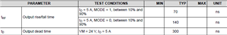
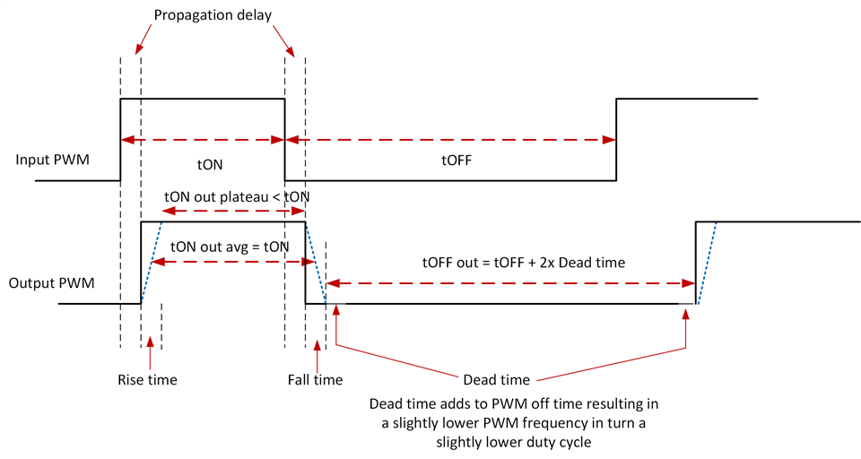
We are using the DRV8962 as 4 independent half bridge drivers, not in H-Bridge config. I assume the effective Ton/ Toff will be Ton/ Toff minus the delay time contributed by propagation delay + rise/fall time + dead time. And the effective duty cycle will be Ton/( Ton + Toff) after minus the delay times.
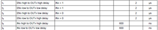
The confusion comes from whether t5/t6 include the rise/fall time and dead time. I did not take t1/t2/t3/t4 into consideration assuming enable pins are already enabled long before switching.
Teffective = Ton/ Toff - t5/t6 since tRF and tD are included in t5/t6
Teffective = Ton/ Toff – (t5/t6 + tRF + tD) as tRF and tD are excluded in t5/t6
Please let me know if any of the above understanding is incorrect. Thank you.