


Other Parts Discussed in Thread: UCC3626
Tool/software:
The datasheets for all versions clearly define operational modes in a set of tables.
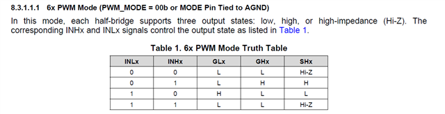
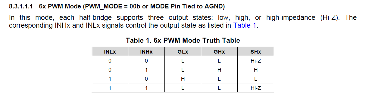
Table 1 describes a simple gate driver mode, where the INHx and INLx signals determine the gate outputs and motor winding voltages. When both INHx and INLx are low (or both are high), GLx and GHx are low and SHx are HiZ.
Question: In this condition, does this mean the gate-to-source voltages for both the high-side and low-side MOSFETs are low, ensuring both MOSFETs are turned off? If both are off, is this why the motor winding connection (SHx) is indicated to be in a high-impedance (Hi-Z) state?
Additionally, while SHx is in a Hi-Z state, it is still connected to the SHx pins of the 8353. Given that GLx and GHx are both low, and SHx is in Hi-Z, how is it guaranteed that the high-side and low-side MOSFETs remain off for extended durations under these conditions?
Also second Q:
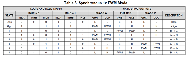
I see that in this mode where Synchronous mode, based on hall conditions, the motor winding that connects to high side of the 3 phase bridge is pwm using both top and bottom fets.. I assume this turns of top then bottom but never together. What is the purpose of this mode? What might be the motor voltages be like. And what applications this is used.
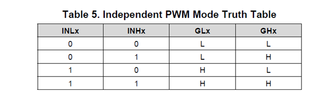
Finally, If I select Table 5. what is the conditions of SHx signals since unlike previous tables it is not defined. What modes table 5 is used? If i hold INHx INLx both low or high indefinitely, will both high and low fets be Off by gate to source voltage both low? and what is the SHx pin of the 8353?

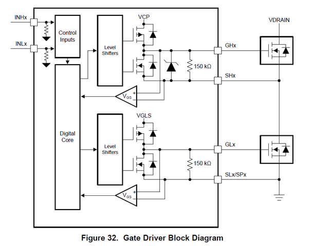

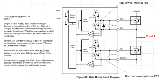
 I_HOLD is the upper-arm or lower-arm internal FET weak current, and I_STRONG is the lower-arm internal FET strong current, with values defined in the DRV835x datasheet here:
  In the example where both INHx was high and INLx was low, then both INHx=INLx= low, it is most likely that both lower-arm internal FETs are on with a weak discharging current (IHOLD) as you suggested, shorting GHX/SHx together and GLx/SLx together, which is HI-Z as we have discussed. And the additional pull-down resistors are implemented to bolster and to help keep the FETs off even when the driver is disabled.