This thread has been locked.

If you have a related question, please click the "Ask a related question" button in the top right corner. The newly created question will be automatically linked to this question.

DRV8847: Current Control

Part Number: DRV8847
Other Parts Discussed in Thread: DRV8718-Q1, DRV8714-Q1

Tool/software:

Hi,

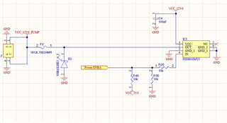
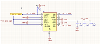
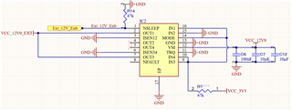
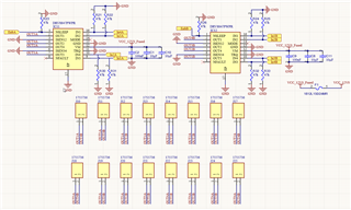
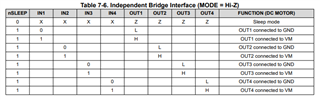
This is my design as shown below. The aim is to have 16 independent latching solenoid drivers, but for some reason, it was not able to output a high voltage of 12V. The maximum voltage being output was 0.7V.

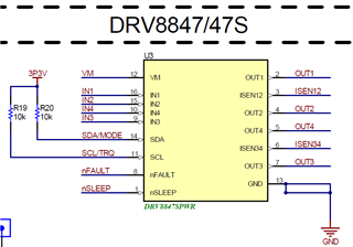
After some investigation, I noticed that ISEN12 and ISEN34 were left floating. As I did not want to limit the current, these were left floating. However, I believe the correct approach would be to connect these to GND. This will be addressed in the next version of the PCB, where they will be connected to GND.

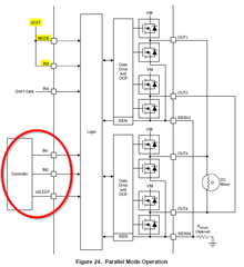
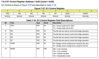
The question I have is regarding the TRQ pin. It seems this also affects the output current. How should this pin be set?

Thank you.

  • Hi,

    Thanks for your question.

    My team mate will review the question and get back to you.

    Thanks,

    Ibinu

  • Hello,

    Yes, you are correct to connect ISEN12 and ISEN34 to GND in order to disable current regulation. The TRQ pin, is used as a scalar input to scale the current regulation threshold. It shouldn't matter whether you connect the TRQ pin high or low as it is just a scalar, but good practice would be to connect it to GND.

    Best,

    David


  • Thank You for your reply.

    Could you explain what advantages this scaler would offer?

    Would there also be a need to include ESD protection on the output pins?

    I have also noticed a small voltage drop on the outputs under load, whereas there was no drop on the actual power supply. Is this behaviour normal for this device? My solenoids draw approximately 0.8A.

  • Hello,

    The torque scaler helps increase the resolution of the current regulation threshold. 

    Adding ESD protection on the output pins is a design choice and would depend on the application. Our device is designed to handle smaller device level ESD strikes, however many system designers include ESD protection on the outputs due to system level ESD strikes are much larger and could potentially cause damage to the device. Please see the following app note on the differences of device level and system level ESD.

    Design considerations for system-level ESD circuit protection 

    When the device switches under load, it is common to see the freewheeling diode drop at the outputs. This voltage drop is expected behavior and is typically around 0.7V.

    Best,

    David

  • Thanks,  So the torque, is better to keep it floating or GND? As I am not limiting my current

    Thank's I will read the application notes

  • Hello,

    It's generally a good practice to tie the TRQ pin to GND. This ensures a stable operation and minimizes the risk of noise affecting the pin. While leaving it floating won't cause immediate issues, connecting it to GND is a safer and cleaner approach. 

    Best,

    David

  • Thank you, I will correct this. I will connect the ISEN and TRQ pins to GND.

    We also aim to use this IC for various applications to increase the purchase quantity for this part and maintain a uniform BOM.

    One of the other applications we intend to use this IC for is to drive a 12V pump, similar to the type used in fish tanks.
    I would like to know:

    1. Can I use multiple pins from the driver for this purpose?
    2. Is there any advantage to connecting the pump to GND via the driver instead of directly?

    In the past, I have used a circuit similar to the one shown below, which includes a protection diode. Am I correct in understanding that this driver already incorporates a protection diode?

    Regarding heat dissipation:
    Since the package is much smaller compared to my existing circuit, I anticipate some heat generation when driving the pump continuously. To manage this, my plan is to connect the GND pad to a copper pour on the top layer, which will be connected via multiple vias to the GND plane. Additionally, the top layer will have a GND plane pour where no signals are present.

    Would this approach be sufficient for heat dissipation? I would like to avoid using a heat sink. The pump is expected to operate continuously for a maximum duration of 6-10 minutes.

  • Hi Dharmesh,

    1. I would like to know which pins you plan to connect together. If you plan to connect the output pins together, this should be fine as long as you don't drive multiple pumps at the same time. I would need to know more information, like are the pumps going to be driven with PWM or just 100% duty cycle ON?

    2. I'm not sure what you mean here, if the pump is being connected from OUTx to GND, then yes it should be connected to the same GND as the device. 

    Correct, you don't need to include a protection diode. The device has integrated freewheeling protection diodes to recirculate the load current during PWM off time. 

    Yes, that sounds like a good plan for heat dissipation. The device will heat up depending on the amount of RMS current the load draws. The datasheet has layout suggestions and power dissipation formulas. 

    Please use the following two app notes for more information. 

    Best Practices for Board Layout of Motor Drivers (Rev. B)

    Calculating Power Dissipation for a H-Bridge or Half Bridge Driver (Rev. A)

    Best,

    David

  • Hi

    I would like to connect more than one pin together—possibly four—to drive a pump. This would increase the current and help mitigate the voltage drop. The goal is to drive the pump at 100% without using PWM.

    Regarding the ground (GND), in a typical H-bridge configuration, one pin outputs VCC while the other connects to GND. What is the advantage of connecting to GND via a pin rather than directly to GND on the PCB? For this application, we don’t require an H-bridge as such and are using the device more as a load switch for the pump. While for my original application, i am firing a solenoid for a max 1 second

    I will investigate the heat effects further, as we plan to run the pump for a maximum of 10 minutes and need to ensure there are no overheating issues.

  • Hi Dharmesh,

    The GND pin from the device should be connected to the GND plane on the PCB - this means there should be no difference connecting from the pin or GND plane on PCB, they will be on the same node. 

    If you don't need the full H-bridge per load, then yes, you can connect multiple loads to the outputs. Each output can be controlled independently using independent half-bridge mode. 

    Best,

    David

  • Hi

    This is how I intend to use it for my other application. All the ENB and signal lines are connected to the same net.

  • Hi ,

    After reviewing the schematic posted above, I see some possible issues that could prevent from connecting the device in parallel mode.

    1. The absolute max ratings for the digital pin voltage (IN1, IN2, IN3, IN4, TRQ, nSLEEP, nFAULT, SCL, SDA) should not exceed 5.75V, its recommended to not exceed 5V for these pins. 

    2. In order to use the parallel bridge interface, both the MODE and IN3 pins need to be connected to an external 3.3V or 5V supply. Then IN1 and IN2 pins can be used to control the driver. 

    From the schematic, MODE is a left floating and inputs are exceeded input voltage range. 

    Please see the datasheet for more information on the parallel bridge interface

    Best,

    David

  • Hi 

    I used the independent mode to drive them all at once. This way, all four output pins can be output compared to only two pins in parallel mode. Is this not possible for this application?

    All the GPIO are 3.3V. The net is called "Ext_12V_Enb", but it is 3.3V

  • Hi Dharmesh,

    No, the device is not designed to be connected in parallel while operating with independent control. There is a possibility of shoot-through if the timing doesn't match up. 

    How much current do you need for the application? 

    Best,

    David

  • Hi

    I need about 1–2A at most, but I am future-proofing my design. At the moment, I do not anticipate any usage above 500mA.

    What you mentioned about timing makes sense, so I have adjusted my design accordingly. I only have one GPIO available to drive this device, so I have configured it to control the sleep mode. The inputs are either high or low, and if they are high, they are pulled up via a resistor. I hope this setup is correct.

  • Hi Dharmesh,

    If the load isn't drawing any more than 500mA, then I'm not sure why you are trying to "parallel the output channels". If using the independent bridge interface, then the MODE pin should be left in the Hi-Z state. 

    The inputs don't need a pull-up resistor.

    Please read the section 7.3.3.4 of the datasheet for necessary connections for the independent bridge interface. 

    Best,

    David

  • Hi 

    At the moment it's only 500mA, but this could increase to 1A or 1.5A as some applications need a little more current to charge a battery. So I was thinking adding two pins would give a little headroom. Therefore the need for a parallel mode I will remove the pull-up resistors and connect directly to 3.3V.

    But just driving the Sleep signal and not Input signals, would that be sufficient I do not see any reason why this would not work, unless the input requires a rising edge?

    We aim to use the same IC in multiple places on our PCB, this way we have one driver IC-type device is going to be used in two different ways on the PCB.

    One is the parallel method as shown in my previous post. and the other is independent as shown in the schematic below: I believe the independent schematic is as per the datasheet.


  • Hi Dharmesh,

    The independent bridge interface schematic looks good.

    Please follow the parallel bridge operation connections in the datasheet for appropriate connections of inputs and outputs. The MODE and IN3 pins need to be connected to an external voltage source, while IN4 is in a don't care state. Inputs IN1 and IN2 are then used to control the outputs. This means the output connections should be as follows in the figure below:

    I suggest using a DRV8847EVM to further evaluate your design. 

    Best,

    David

  • Thanks 

    As my PCB will include approximately three of these ICs, and considering the possibility of future PCB variations with even more ICs, I believe the I2C version could offer significant advantages. This is primarily because it reduces the need for additional GPIOs to drive the devices. If I understand correctly, for each new device added, I would only need one additional GPIO for the nFault configuration. The SLEEP can be common for all the devices if need be.

    I have some questions:

    1. If I don’t require the nFault pins, could I simply keep the address of each device the same and toggle the nFault pin to differentiate between them? Alternatively, if this isn’t possible, I could add this signal and assign a unique address to each device. Does this address reset once the device goes into sleep mode?

    2. Can you confirm whether there is a reference design available for the I2C variant? I believe the additional input pins can be left floating, or should they be tied to GND or 3.3V? Am I correct in assuming that all inputs and modes are configured through I2C?

    3. Is there no thermal pad package available for the I2C variant? If not, how would this impact heat dissipation compared to the other package options?

    4. Based on block diagram 7.2, it shows that SDA requires an external pull-up, while SCL has an internal pull-down. Our PCB typically uses a 4.7k pull-up resistor on the I2C bus. Would this cause any issues?

  • Hi Dharmesh,

    If I don’t require the nFault pins, could I simply keep the address of each device the same and toggle the nFault pin to differentiate between them? Alternatively, if this isn’t possible, I could add this signal and assign a unique address to each device. Does this address reset once the device goes into sleep mode?

    The nFAULT pin on the DRV8847S (I2C device), is used as an input to release the I2C bus. I'm not sure if only one nFAULT signal is toggled at once this could work, because I'm not sure what state the other devices would be in while one is selected. They could be tricked into thinking a fault has occurred if they get pulled low. I would recommend testing first. Assigning unique addresses for each device is the recommended approach. 

    Can you confirm whether there is a reference design available for the I2C variant? I believe the additional input pins can be left floating, or should they be tied to GND or 3.3V? Am I correct in assuming that all inputs and modes are configured through I2C?

    The DRV8847SEVM can be used for testing. Input pins will still be needed to control the outputs, the I2C communication is used to change the register settings within the device. Please refer to the datasheet and EVM User's Guide for more information on programming and device configuration. 

    Is there no thermal pad package available for the I2C variant? If not, how would this impact heat dissipation compared to the other package options?

    No, there is no thermal pad for the I2C variant. Power dissipation calculations are covered in the datasheet for estimated losses. 

    Based on block diagram 7.2, it shows that SDA requires an external pull-up, while SCL has an internal pull-down. Our PCB typically uses a 4.7k pull-up resistor on the I2C bus. Would this cause any issues?

     A 10k pullup resistor is used for both SDA and SCL. Please see the hardware files on the EVM product page for more connection information used on the DRV8847SEVM.


    Best,

    David

  • Thanks 

    I might be wrong but in the datasheet it shows you can set input pins via the reg.  

    Instead of purchasing a eva kit it would be more better to get the PCB made, but want to make i2c will work instead of using gpio pins

  • Hi Dharmesh,

    My mistake. Yes, you are correct. It looks like you can use the IC1 Control Register to control inputs. 

    Best,

    David


  • I got my board working with i2c

    Is it possible or any compatible device, where I can also output a High Impedance in addition to a High and Low output per pin, instead of a pair?

  • Hi Dharmesh,

    With independent half-bridge control, you can control each output independently, however, this won't be possible while in parallel mode. 

    Best,

    David

  • HI

    I can control each output only for high and low, but how do I set it for high impedance? 

  • Hi Dharmesh,

    The nSLEEP pin must be pulled low to put the outputs into a Hi-Z state.

    Best,

    David

  • Is there away i can have only one GPIO in High z , while the other is in Low or High? Or is there any device that can do that?

  • Hi Dharmesh,

    This won't be possible while in independent half-bridge mode. Most of our industrial devices, while in independent half-bridge mode, require nSLEEP to be pulled low. 

    We do have devices like the DRV8714-Q1 and DRV8718-Q1 that can do this operation; however these parts are a bit more complicated and are gate drivers. 

    DRV8714-Q1 data sheet, product information and support | TI.com 

    DRV8718-Q1 data sheet, product information and support | TI.com

    Best,

    David