DRV8770: DRV8770RGER Design Questions

Part Number: DRV8770

Tool/software:

Dear Texas Instruments Support Team,

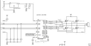
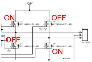
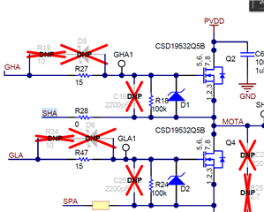
I hope this message finds you well. I am currently working with the DRV8770RGER motor driver and have a few questions regarding its operation. Specifically, my design which is attached to this message.

Could you kindly provide the following information:

  1. What are the ideal input voltage and current levels that should be applied to INHA, INLA, INHB, and INLB to correctly trigger the outputs on the DRV8770RGER?
  2. Are there any specific conditions or limitations that should be considered for these input pins to ensure proper functionality relating to my design?

Additionally, I would appreciate your input on whether my current design, based on these parameters, aligns with the recommended operating conditions for the device. I want to ensure that the setup is optimal for the efficient and reliable performance of the motor driver.

Thank you for your time and assistance. I look forward to your response.

  • ,

    1. The pins voltage and current levels are detailed in the datasheet under Section 6.5 Electrical Characteristics. Each parameter is listed with min, max, and typical values all specified under labeled test conditions. 

    2. The input pin connections look good. However, the input pins already have integrated pull down resistors, so they are not necessary. 

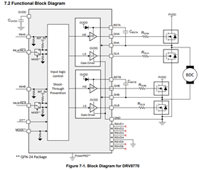
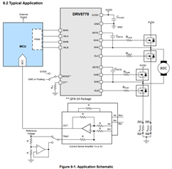
    I would also suggest looking at Section 8.2 Typical Application of the datasheet as it shows a suggested layout and connections to follow. 

    Best,

    David

  • Thanks for the initial reply.

    With my current design i have an input signal 

    INHA - LOW

    INHB - HIGH

    INLA - HIGH

    INLB - LOW

    GVDD =14.97

    MODE- FLOATING

    DEAD TIME RESISTOR - 82K 

    My output signals are:

    GLA-ON

    GHB-OFF

    GHA-OFF

    GLB-OFF

    boost a and boost b -14.3v

    are there any reasons why GHB is off?

  • Hi Michael,

    It seems like is functioning properly while channel B is not. Looking at the logic inputs, the INHB = 1 and INLB = 0 should enable the high-side FET but instead the outputs are in an invalid state. 

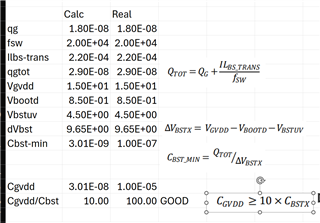
    It's always a good idea to review the bootstrap capacitor selection section of the datasheet to make sure the cap value is large enough. 

    The dead time resistor is set to 82k, which should make the dead time between the high-side and low-side FETs around 410ns. Is this what you are seeing for channel A?

    Are the inputs switching at some PWM frequency, or static?

    Best,

    David

  • Hi David,

    Thanks again for your continuous assistance 

    The photo attached above is my calculation for the bootstrap capacitor and everything satisfies the requirements on the datasheet. 

    Yes, i have a deadtime of about 12ms switching from channel a to b and the inputs are switching with a frequency at 20kHZ.

  • Correction:  The inputs are static for my tester..

  • Hi Michael,

    Please allow me 24 hours to review the calculations and schematic. I'll have more information by tomorrow. 

    Best,

    David

  • Hi Michael,

    If possible could you provide scope captures on input and output signals?

    It looks like the load is trying to be driven in the reverse direction, I would recommend driving it in the forward direction. 

    Have you tried replacing the Q4 FET? If the driver is able to drive in forward direction, maybe we can isolate the issue to the external FET.

    Also, have you tried evaluating the device on the DRV8770EVM? If not, it's always recommended for new designs. 

    Best,

    David

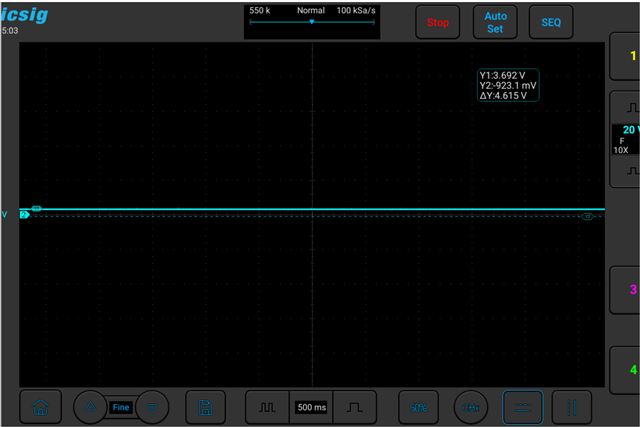
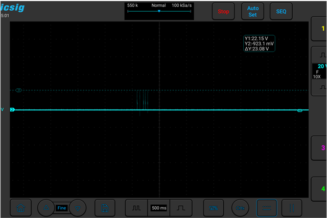
  • 3.3V input voltage on INLA and INHB (Reverse Direction)

     Q12 Gate Voltage (Reverse Direction).

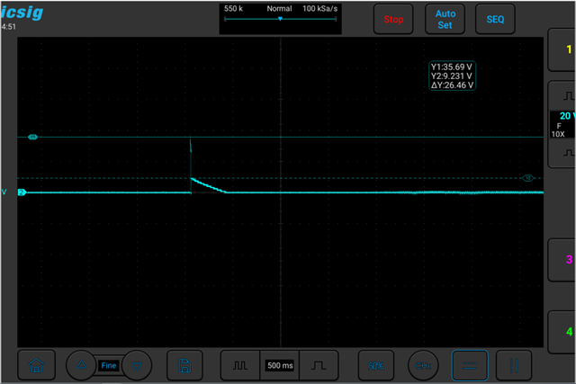
    Q6 Gate Voltage (Reverse Direction).


    3.3V input voltage on INHA and INLB (Forward Direction)

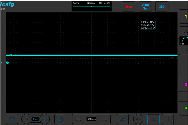
    Q11 Gate Voltage (Forward Direction).

    Q8 Gate Voltage (Forward Direction).

  • These are the signals i get when i instantly apply 3.3v to two inputs, this is the Mosfet i use -(MCAC38N10Y-TP). i have tried replacing the Mosfets but nothing changes. After driving in both directions i see that both high side Mosfets are not getting power. Yes i prototyped with  DRV8770EVM before designing the board and it worked.

  • Hi Michael,

    What's the GVDD and PVDD voltages? Are you expecting to see 15V at the gate?

    Best,

    David

  • GVDD is 15v and PVDD is 24v. Yes, I'm expecting to see 15v at the gate.

  • Hi Michael,

    The DRV8770EVM uses a 100kΩ resistor connecting from gate to source on both high-side and low-side for a stable voltage level and to prevent a possible floating gate voltage level. The Zener diode (16V) is optional but also there to clamp any transient voltages higher than 16V in order to protect the FET.

    Also the pulldown resistor on the input pins isn't necessary as they already have 200kΩ internal pulldowns. 

    Best,

    David

  • Hello David,

    unfortunately, after adding the diode and resistor that didn't fix the issue. I also tried just sending 3.3v into the inputs individually and on the gates of my low side I get 15v, on the gates of my high side I get 1.292v. Any other suggestions would be appreciated.

  • Hi Michael,

    Please allow me some time to review and I'll reach out with some suggestions. 

    Best,

    David

  • Hi Michael,

    After reviewing the issue, I have a few more suggestions. 

    1. It's possible the high-side FETs are having trouble turning on could be due to the limited amount of time the bootstrap capacitor has to charge. In order for Q11 to have enough gate charge to turn on, Q12 must be conducting for a minimum pulse width to charge the bootstrap capacitor. 

    The minimum input pulse width on INHx, INLx that changes the output on GHx, and GLx is specified in the datasheet as tPW_MIN which is typically around 70ns. I would suggest pulsing INLx for the maximum recommended value of 150ns to be sure the capacitor has enough charge. 

    2. I would also review calculations to be sure that the local GVDD bypass capacitor is greater than the bootstrap capacitor, by at least 10x.

    3. The gate resistance of 10Ω on GHx and GLx should be fine, but it could also be worth it to review the Gate Resistance Selection of the datasheet and maybe try increasing it to change the slew rate on the SHx pins. 

    Gate Resistance Selection (datasheet) 

    Best,

    David

  • Thanks David, this solution solved my problem.