Tool/software:
It is possible to use the DRV8351 to switch a GaN?
The DRV8351 has a Gate Driver Supply of 5-15v and the GaNs VGS is +6 / -4. So I assume this will work.
Are there any other parameters I need to consider to make this work?
This thread has been locked.
If you have a related question, please click the "Ask a related question" button in the top right corner. The newly created question will be automatically linked to this question.
Tool/software:
It is possible to use the DRV8351 to switch a GaN?
The DRV8351 has a Gate Driver Supply of 5-15v and the GaNs VGS is +6 / -4. So I assume this will work.
Are there any other parameters I need to consider to make this work?
Hi Lachlan,
I'm actually not sure, let me check with my team. I'll have an update tomorrow
Regards,
Yara
Hi Lachlan,
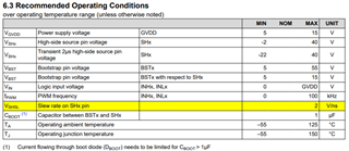
The datasheet specifies that DRV8351 is meant to drive NMOS (N-channel power MOSFETs). NMOS slew VDS voltages much slower than GaN-targeted applications. Too high of an SHx slew rate can result in electrical overstress.
What is the reason behind selecting GaN HEMT?
Regards,
Yara
Thank you, Yara.
We selected GaN HEMTs for their high efficiency and smaller size and weight. However we are open to using MOSFETs if GaN are not able to be driven by the DRV8351. Are there any options to reduce the high slew rate to prevent electrical overstress? or will reducing this make it not worth using GaNs in the first place?
Thanks
Hi Lachlan,
The significantly faster switching speed is definitely a big selling point for GaN HEMTs so I think if you're not able to take advantage of that then it'd be good to stick with NMOS.

DRV8351SEP specifies the maximum SHx slew rate is 2V/ns (This is best case scenario with optimal layout design, I would actually stay around 0.5V/ns - 1V/ns to really avoid any issues with SHx)
Regards,
Yara