This thread has been locked.

If you have a related question, please click the "Ask a related question" button in the top right corner. The newly created question will be automatically linked to this question.

DRV8411A: Max continuous current

Part Number: DRV8411A

Tool/software:

Hi All!

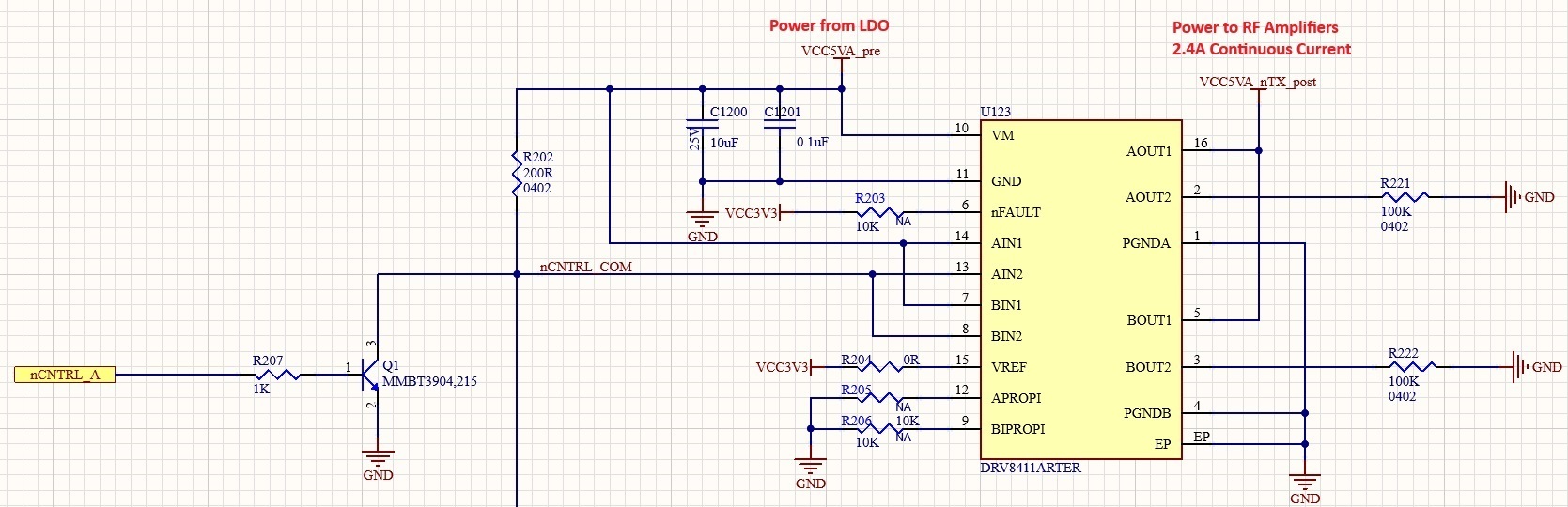
In my application i need to deliver 2.4A continuously from 2 channels and sometimes to shut them off. The VM voltage is 5V

In the datasheet it is stated the peak current is 4A.

 Is this max current can be achieved when paralleling the 4 channels or it is for each one of them?

 Can i use this device for my application?  

Best Regards,

Yonatan.

  • Hi Yonatan, 

    The DRV8811A peak current is 4A. The rms (average) current is determined by the thermal considerations of the IC. The rms current is calculated based on the RDS(ON), rise and fall time, PWM frequency, device quiescent current, and package thermal performance in a typical system at 25°C. The actual operating rms current may be higher or lower depending on heatsinking and ambient temperature. By considering all factors the IC should work fine under 2.4 under parallel bridge interface.

    Best regards, 

    Mojtaba

  • Hi Mojtaba !

    How are you?

    This is the setup I'm using:

    Is this correct in order to transfer 2.4A continuously?

    Is it necessary to add resistors to prevent shoot through situation?

    Best Regards,

    Yonatan.

  • Hi Yonan, 

    Thank you for updating information. The schematic looks fine. 

    Is this correct in order to transfer 2.4A continuously?

    Please refer to Thermal Considerations section 9.1.1.3 for detail explanation. 

     https://www.ti.com/lit/ds/symlink/drv8411a.pdf?ts=1740597120835&ref_url=https%253A%252F%252Fwww.ti.com%252Fproduct%252FDRV8411A

    The Maximum Output Current of a motor driver is a function of die temperature. This, in turn, is greatly affected by ambient temperature and PCB design. Basically, the maximum motor current will be the amount of current that results in a power dissipation level that, along with the thermal resistance of the package and PCB, keeps the die at a low enough temperature to stay out of thermal shutdown.

    Total power dissipation for the device is composed of two main components. The power MOSFET switching losses, and the power MOSFET RDS(ON) (conduction) losses.

    PTOT = PSW + PD

    PSW = PSW_RISE + PSW_FALL///   PSW_RISE = 0.5 × VM × IRMS × tSR × fPWM ///   PSW_FALL = 0.5 × VM × IRMS × tSR × fPWM 

    PD = (IRMS) 2 × (RDS(on)High-side + RDS(on)Low-side)

    The device had an effective thermal resistance RθJA of 45°C/W. The junction temperature TJ value becomes:

    TJ = TA + (PTOT × RθJA)

    The actual system performance may be better or worse than this value depending on PCB stackup, routing, number of vias, and copper area around the thermal pad.

    Is it necessary to add resistors to prevent shoot through situation?

    It depends on your application. 

    Please let me know if you have any questions. 

    Best regards, 

    Mojtaba.

  • Hi, thanks!

    I'm not working with PWM so I don't have switching losses. Correct?

    P.S... in the schematic above i use the component as a power switch which connects and disconnects the main power (VM pin) to the Load (AOUT1, BOUT1 Pins)

    according to its control pins (AIN1, BIN1, AIN2, BIN2)

    Best Regards,

    Yonatan.

  • Hi Yonatan, 

    Thank you for your questions. 

    I'm not working with PWM so I don't have switching losses. Correct?

    If it is on/off switches, you can ignore the switching loss. 

    Please let me know if you have any questions. 

    Best regards

    Mojtaba