This thread has been locked.

If you have a related question, please click the "Ask a related question" button in the top right corner. The newly created question will be automatically linked to this question.

DRV8353F: Considerable Commutation Confusion

Part Number: DRV8353F
Other Parts Discussed in Thread: DRV8353, CSD19536KTT, UCC27301A

Tool/software:

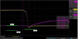
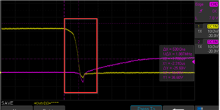
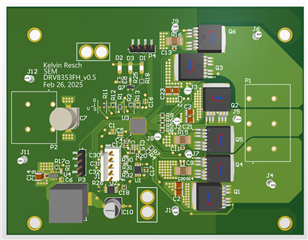
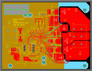
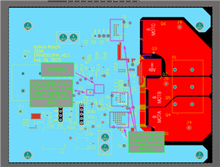
Hey everyone, I hope you're doing well. I have a question about BLDC commutation on the DRV8353F. I'm bringing up a motor controller that I built. It currently runs at 36V, and this scope trace was taken while running 0.5 A, but I will get it up to 48V 40A eventually. In the scope picture, pink is the lowside gate, and yellow is the highside gate for one of the phases.

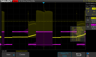
Before the PWM commutation step, the highside gate PWM at a lower voltage, and the lowside gate remains low. From what I understand, the highside gate shouldn't be PWM-ing in this phase. Here's a chart of what I think BLDC commutation should look like:

Good commutation example

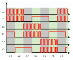
Let's say in my oscilloscope I'm measuring the B phase. I don't understand why, in commutation step AC (the second one), it looks like B+ is PWM-ing on my oscilloscope capture. I checked the other two phases, and they also look the same. Is this what the gate lines are supposed to look like? According to the commutation table (Table 8-3) on page 23 of the DRV8353 datasheet, it doesn't look like my highside gate should be doing anything in this phase. Also, I doubt it's a hall sensor issue because if I were in a commutation state for that phase, the lowside gate would be switching as well, but only the highside gate is being switched here. 

I'd be really grateful for any advice or support here. 

Thank you for taking the time to read this.

Cheers,

Kelvin

  • Hi Kelvin,

    How are you measuring your signals?

    Can you measure and post GHx to SHx, SHx to GND, GLx to GND, and you input signals?

    Regards,

    Yara

  • Hey Yara, here are some scope traces:

    GLA and SHA with respect to (wrt) GND:
    https://cornell.box.com/s/b7a81b1lzm7g37uzofqkf3n64uh0f9jp

    GHA wrt SHA while commutating:
    https://cornell.box.com/s/tc46ecmxx98r1avewnrme76njjdlukon

    GHA wrt SHA at the very beginning of the back emf phase:
    https://cornell.box.com/s/h1iwl6knhkc3x0tjqmk5eajggltv3pls

    GHA wrt SHA in the middle of the back emf phase:
    https://cornell.box.com/s/5vctp1sf3opdkgxu7rcz1ikdrv5jwwkr

    GLB and SHB wrt to GND:
    https://cornell.box.com/s/k33zt2mpzhf9wzv7dfumq821peao4wq7

    GLB and GHB wrt to GND:
    https://cornell.box.com/s/5zux34h9z0npya24umioovqil97se41t

    I realized I was being really silly and I was looking at the back emf of my motor. But why is there no back emf on the other side of my commutation? It's just zero. I feel like that's weird. This is a picture of GLA and GHA during a few electrical periods.
    https://cornell.box.com/s/rj5bflcxv6b80fk2w68c1codtc7m7p2m

    You can see GHA get pulled up to the SHA in one of the back emf phases through the internal diode of the gate driver, but this doesn't happen on the phase after the two PWM phases. By the way, I'm using the word "phase" to describe one of the six commutation steps that a BLDC motor goes through, depending on the hall sequence. Let me know if I'm using the wrong word. 

    Anyways, can you tell me why I don't see any backemf after the PWM phase?

    Cheers, 
    Kelvin.

    PS, I have a question about my picture of GLB and SHB wrt to GND (https://cornell.box.com/s/rj5bflcxv6b80fk2w68c1codtc7m7p2m). Why does SHB slew downwards before GLB's voltage increases? And why does GLB dip downwards? What's pulling SHB down if GLB hasn't even increased yet? I'm a little confused by this, but I think it's because my FETs have a big Crss (760 pF), and a lot of current is flowing through Cgd. Like more than the high-side FET of the gate driver can provide, so I'm getting current through the low-side body diode of the gate driver and also current through Cgs. I definitely could be wrong tho. Take a look at my picture from "Understanding Smart Gate Drive" for a better explanation:
    https://cornell.box.com/s/z65o4r4hc0dozmr7fbiehx14a61ph96c

    I'd appreciate any input!

  • Hi Kelvin,

    Thanks for the waveforms! I think I may be missing the trace labels however I think its still giving me a better idea of what is potentially going on.

    What are the MOSFETs being used? Do you have a datasheet? and what IDRIVE setting are you using?

    I see a few instances in the waveforms that you've provided that could indicated the Qgd of your MOSFET might be too small for the IDRIVE setting you've selected

    On a few of the waveforms there looks like there was ringing whenever the gate is switching, this ringing can couple into the other side (ringing on high side couples into the low side or vice versa)

    It would be helpful to see the outputs of one phase all on one scope if you have the channels for it? Here's an example:

    No need for the current output, only GHA-SHA, SHA to GND, and GLA to GND (if you only have two probes measure SHA to GND and GLA to GND on one waveform and GHA-SHA and GLA to GND on another). Try to get a zoomed in shot of this section:

    Regards,

    Yara

  • Hi Kelvin,

    I also forgot to ask if you can directly upload the images here instead of linking them? TI network restrictions sometimes interfere with me being able to access these links.

    Regards,

    Yara

  • Hey Yara, sure, I'll put the files in directly now. 

    I'm using IRFS7530-7PPbF MOSFETs. Here's the datasheet:
    Infineon-IRFS7530-7P-DataSheet-v01_01-EN.pdf
    I'm using 50/100 mA IDRIVE in this picture because my gate driver keeps breaking with a hard short GLx to GND and soft short 1k Ohms VGLS to GLx when I have higher IDRIVE values. The motor attached to the board is pulling 0.6-1.0 A in these scope traces, but I'm trying to make it more. 

    My Qgd is 73 nC, which is a lot compared to similarly-sized FETs that I've seen from TI, like the CSD19536KTT from TI's reference design (https://www.ti.com/tool/TIDA-010056). 

    As for the scope traces, I broke my motor controller because I set IDRIVE to 150/300 mA up from 100/200 mA, and the GLB shorted immediately, so please bear with me while I solder a new one.

  • Hi Kelvin,

    That's pretty interesting, typically with ringing like your seeing in these scope shots more often then not its because Qgd is too small and IDRIVE setting is too high. The Qgd of your MOSFET is quite large, I'd expect you to be able to use anywhere from 200mA to 700mA (if your layout is good)

    Can you provide a screenshot of your layout around the output pins and traces? and measurements of the width of the traces? Feel free to post your schematic as a pdf as well for review.

    Regards,

    Yara

  • Hey Yara, I have really bad trace inductance here because I split my ground planes into a power ground and signal ground (horrible idea, the internet lied to me). Here is my board:

    Here is the top layer:

    Here is the ground plane with the ground return loops for the low side gate drive circuit mapped out:

    And here is the power plane, which is supposed to be 48V.

    So I redesigned my board to make a solid ground plane and also increase density:

    The increased density should help a little with trace inductance, but I think it's effect is small compared to getting rid of my split grounds (again, terrible idea)

    In both cases, my gate drive traces are 30 mil. v0.5 (the second, better version without the ginormous return path) hasn't come in yet, but I have some pretty good evidence that the lack of backemf in the second half of the scope trace above is because there is mutual inductance between my gate drive traces causing the low side FETs to turn on when they should be in the high-impedance step of commutation. This pulls the SHB line low when it should be Hi-Z. I'm pretty sure of this because Q5 (the lowside phase B FET) was getting really hot (80C) even at low motor current (1 A), I can see voltage coupling between the Q5 gate and SHA (so maybe it's capacitive coupling, but I'm pretty sure it's inductive), and when I added gate resistors, Q5 stopped getting hot. I know this isn't super clear, so I'll make a follow-up post with data and pictures and better explanation, but the lowside FET internal to the DRV8353 gate drive output for the lowside power MOSFET shorted to ground before I was able to get data.

    If you could review my schematic, I'd really appreciate any comments at all because I work in a university car team, and the E2E forums have been really helpful for all our team members, including underclassmen, to learn how to approach debugging electrical systems.

    v0.5 Schematic.pdf

  • Also one more thing, just FYI, I made another revision last week where I put external gate drivers (UCC27301A) on the output of the DRV8353. The external drivers are 4.5 A source and 3.7 A sink, which should hopefully not keep breaking via hard short on the gate drive output to GND. I'll update with results when the board comes in because it might be cool. Here's the schematic for it. 

    v0.6 Schematic.pdf

    The main changes to this are the gate drivers, and that I had to short the SHx pins to ground so that they don't get bootstrapped to VDrain, since the DRV8353 gate drive outputs are now inputs to the external gate drivers.

  • Hi Kelvin,

    Give me a couple of days to look over the layout and schematic, thanks for all the info!

    Regards,

    Yara

  • Awesome thanks so much Yara

  • Hi Kelvin,

    Your second layout is definitely going in the right direction, I'm curious to see the results once you test!

    A few things I wanted to mention:

    1.

    I split my ground planes into a power ground and signal ground (horrible idea, the internet lied to me).

    The internet might have had some truth behind what it told you.

    Did you have a net tie between PGND and AGND? This allows an intentional connection of both ground and helps avoid unintended loops.

    We have some pretty good resources regarding layout design: 

    https://www.ti.com/lit/an/slva959b/slva959b.pdf?ts=1710808643945&ref_url=https%253A%252F%252Fwww.google.com%252F (read the Grounding Optimization section)

    https://www.ti.com/lit/an/slvaf66/slvaf66.pdf

    I realize you just redesigned your layout, but these are still good references if you decide to redesign again.

    2.

    Try to make your power stage symmetrical. A good reference for this would be some of our gate driver EVMs, you can access the design files on the EVM webpage

    https://www.ti.com/tool/DRV8353RH-EVM

    also I see that your vias are not going under your MOSFETs, this could be the reason why your MOSFETs are heating up:

    Here is how the DRV8353 EVM MOSFET vias are placed:

    The MOSFETs also have multiple layers to help dissipate heat.

    3.

    I'm a little confused on your application of UCC27301A. I haven't really seen this design before, DRV8353 is a gate driver, UCC27301A is also some kind of gate driver (not really familiar with this device, its not considered a BLDC so my team doesn't manage this one) So it kind of looks like your using our gate driver to driver another gate driver?

    Also in your schematic the "MODE" resistor is labeled as "do not populate", does that mean it is tied to GND or left floating?

    I see you have multiple LDO circuits as well? Why not just use DVDD as 5V LDO?


    In conclusion, you should really consider adding vias and more polygon pour layers under your MOSFETs if you're dealing with overheating MOSFETs. Please take advantage of the app notes I linked and the EVM design files.

    Regards,

    Yara

  • Yara, thanks so much for your feedback. I really appreciate it. A few questions to clarify:

    Ground partitioning:

    I've read both of these a few times actually. They were super helpful. However, my issue was that I physically separated my signal and power grounds and joined them at a single point, causing a big loop in my ground return path. In the app note "Best Practices for Board Layout of Motor Drivers (Rev. B)"  Section 1.1 > Partitioning, it just says that "This separation is not a physical partition of digital and analog ground," which is what I did. So to confirm, for motor controller design, partitioning the ground plane does not mean physically dividing the ground plane at all, right?

    Vias under MOSFETS:

    Doesn't this wick away solder from the pad causing a bad bond between the drain pad on the package and the pad on the PCB?

    UCC27301A:

    Yeah, this is a half-bridge gate driver. I'm using the DRV8353 as a logic chip instead of as an actual gate driver. So I'm mostly just using it for the HALLx and 1xPWM lookup table. It's definitely using a gate driver to signal another gate driver, though. 

    I used multiple LDO circuits because DVDD only has a 10mA max output current, and I don't know how much the halls draw. I'm sure the current draw is like nothing, but I'm not going to optimize for parts/cost until the motor controller works. Using a beefy LDO for the 5V just eliminates a possible failure mode. I'll probably try removing it once I get a good motor controller design.

    If you don't think the vias would wick away solder from the pad, then I'll add vias underneath in future revisions. I'll also add the extra layers as well. Thanks so much for taking the time to look at my design. I really appreciate it, Yara!

  • Hi Kelvin,

    Here is kind of a rough depiction of what a split ground could have looked like your layout (the green and blue highlight). Its best to have large solid pours, the AGND plane in your original layout was bottle necked right at the device. How did you originally join the two ground planes? where was the single point you mentioned?

    In our EVM designs that do have split ground we typically join the two grounds using a net tie close to the DRV.

    Doesn't this wick away solder from the pad causing a bad bond between the drain pad on the package and the pad on the PCB?

    This is a valid concern, but I think as long as you place the vias evenly spaced out kind of how its demonstrated in the app notes you shouldn't have any issues.

    Regards,

    Yara

  • Hey Yara, thanks so much for the advice. That makes some sense. I'll come back to this ground plane discussion when I finish testing these new boards and redesign the system. I'm also thinking about using a different 4-layer stackup. I use Signal/GND/PWR/Signal right now, but I'm thinking about using Signal+PWR/GND/GND/Signal+PWR if I find any issues with signals on the back layer caused by low capacitance between my PWR and GND planes.

    Speaking of which, the new boards came in, and I soldered one tonight and tested with IDRIVE = 50/100 mA, and R_g = 10 ohms. I know the DRV8353 uses smart gate drive, and it says that I shouldn't use gate resistors unless I have some sort of automotive EMC compliance thing, which I definitely don't have, but seeing as the IC kept breaking with a hard short to ground on the GLx pin, I'm putting some padding for safe measure, so long as I don't see shoot-through issues.

    I do, however, seem to have dV/dt turn-on issues on the rising edge of SHx during the backemf phases. I know that the DRV8353 has a strong pulldown during the commutation phase when the high-side FET switches, which pulls SHx high very quickly, but I don't think this pulldown happens when a phase is experiencing backemf, even though SHx seems to slew pretty rapidly in this phase as well. I'm going to test more in detail tomorrow, but I just wanted to ask you if GLx gets a strong pulldown during the backemf phase, or if GLx is high impedance here. 

    This matters because when SHx is on its rising edge, GLx will couple through Crss (aka Cgd), and the gate voltage will try to rise. If the half-bridge for GLx is high impedance, then the gate voltage will be allowed to rise during the backemf, and you can get dV/dt turn-on, which I think I might be getting. Inversely, when SHx is on its falling edge, GLx will coupling through Crss (aka Cgd), and the gate voltage will try to go negative. If the half-bridge for GLx is high-impedance, then GLx will get clamped to roughly -0.7V by the body diode of the low side FET inside the DRV8353, but this is bad because body diode conduction is inefficient. If GLx is active low, then the DRV8353 will supply current through the lowside FET, and that's probably fine.

    Let me know if this concern makes sense to you, and if you know what state GLx is in during the backemf phase. I'd really appreciate any info. Thanks Yara!

    PS I've been looking at Hector Hernandez's PCB project for the DRV8353RX EVM, and it's awesome. You guys are awesome.

  • Hi Kelvin,

    It's not uncommon to use gate resistors even in non-automotive application, always good top at least design in the option to have a gate resistor. I will say though you should only use the gate resistor to kind of fine tune IDRIVE and not heavily rely on it.

    From what I understand about the DRV8353, the strong pulldown on GLx (low-side gate drive) occurs during active switching events, but during the freewheeling/back-EMF phase, GLx is in a high-impedance state. This means that when SHx rises due to back-EMF, the voltage can capacitively couple through Crss and potentially turn on the low-side FET unintentionally. This dV/dt turn-on can lead to shoot-through, which might explain some of the failures you’ve experienced.

    You are also using a MOSFET with a pretty high Qgd (73nC if I remember correctly?) higher Qgd means you need more charge to fully switch states which means more charge is able to couple into GLx, this could be the reason behind why GLx is trying to turn on while it Hi-z

    Regards,

    Yara

  • Yara you are the GOAT. There's a pair of DRV8353 chips in this car
    https://www.youtube.com/watch?v=vuXSnx9sw_4

  • I'll continue to optimize the controller and I'll come back to this thread with how I fixed some issues in case other people run into the same things too, but I just wanted to let you know that I'm really grateful for all of your help here.

  • Hi Kelvin,

    Thanks for sharing the video, that's awesome! Glad I could help and you were able to find a lot of your answers here on E2E Slight smile

    I'll be closing this thread but feel free to start another thread when you have an update and link this thread to it or simply reply to this one (you might not be able to reply to this one after 30 days have passed since the start date of this thread)

    If you do redesign your board, post it on E2E for review before you get it built so we can provide feedback.

    Great job on your project!

    Yara