Tool/software:
Hi Team,
Regarding this E2E thread
Customer do more tests to reproduce the GLA short to ground fault.
They are use 3X control mode, and they test with external Cgs from 4.7nF to 10nF, higher Cgs, higher probability to trigger the short.
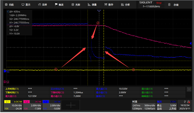
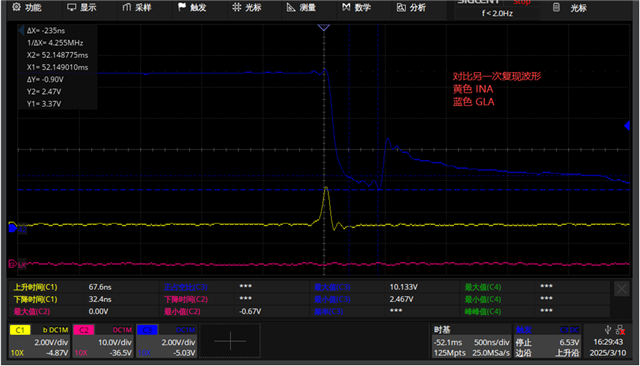
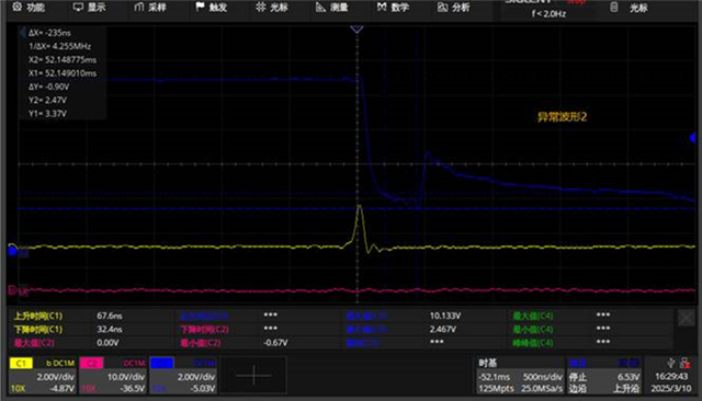
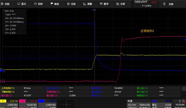
Yellow: INA, Blue:GLA, RED:GHA
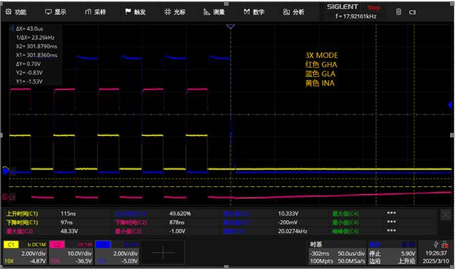
Fault figure 1:

Fault Figure 2:
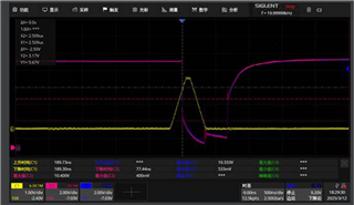
Normal figure 1:
As we can see in the fault figure, in very narrow pulse of INA, the GLA will short to ground in the falling edge, customer don't think is the negative voltage issue.
Please help to found the root cause.
Thank you,
Yishan Chen