This thread has been locked.

If you have a related question, please click the "Ask a related question" button in the top right corner. The newly created question will be automatically linked to this question.

DRV8718-Q1: Amplifier output & nfault pin

Part Number: DRV8718-Q1

Tool/software:

1. From my understanding, for the internal amplifier output, there should be one C-R-C circuit, is it right?

Do you have the recommendation value?

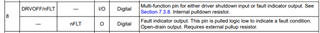
2. For DRVOFF and nFault Pin, if it is configurated as nfault.

How the customer should turn off/Shutdown (All channel driver output low) the DRV8718?

If there is not switch in the Vbat circuit. 

  • Hi. 

    Thank you for you questions.

    1) If CSA blanking function is not used, this discussion is not valid. Most of customers do not use this- CSA blanking is optional. I may suggest to put around 5Kohm + 10nF, CSA_BLK disabled, then try how looks like.

    2) nSLEEP is man "shut down device" pin. DRV will be sleep mode while nSLEEP = Low.

    regards

    Shinya

  • For the sleep status:

    Whether the bottom bridge driver is still turn on?

    another question is about the brake circuit:

    R19 is 1M. But the leakage current of D6 could be several uA, so the voltage could be several Volt, whether there are some risks?

  • Hi,

    Thank you for your questions. Will feedback to you in 24hours.

  • Hi,

    During sleep state, bottom side of driver is turned off. GL5-8 has semi-active pull down, then external low-side FET are turned off.

    GL-1-4 also has passive pull down. Therefore, external low side FET are turned off.

    BRAKE pin's abs max is PVDD. R19 can be reduced if needed. Then drawback is increasing leakage current from PVDD. R19 of 1Mohm is just example.

    Please generate new post when you ask new questions from next time. Thank you for understanding.

    regards

    Shinya