This thread has been locked.

If you have a related question, please click the "Ask a related question" button in the top right corner. The newly created question will be automatically linked to this question.

DRV8844: Over current protection (OCP) not tirggering properly during stall test

Part Number: DRV8844

Tool/software:

Hello,

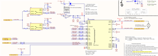
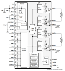
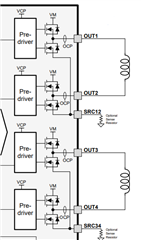
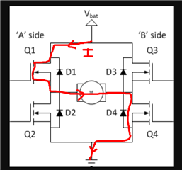
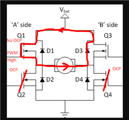
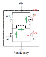
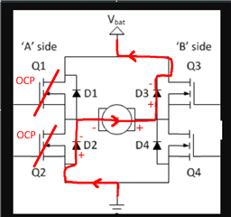
We are currently using the DRV8844 in order to drive a DC motor with slow decay. We are connecting the two outputs of the driver in parallel in order to increase the maximum current that can be drawn from the driver.

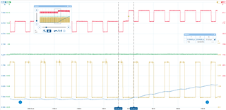
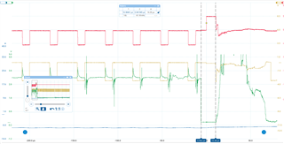
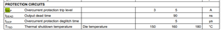
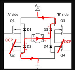
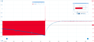
For our test, we are driving the motor with a PWM 48V @ 32kHz  with a duty cycle 30%. The motor is stalled shortly after startup. As shown in the picture below, the output PWM (red) is applied, and the current (blue) is increasing up to a maximum value of ~8.64A. This value seems already quite high, since the over-current protection is supposed to trigger at 5A. At the failure, a spark is visible on the chip, and it is unusable afterward.

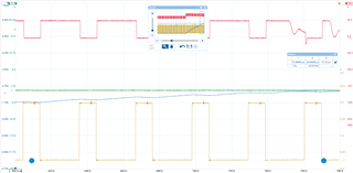
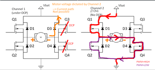
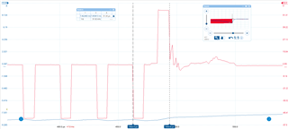
Let's zoom in at the time of the failure. We can observe that the PWM is performing its job properly. When the current is at its highest value, we observe an inversion of the voltage applied to the motor. The failure occurs when the PWM should go low again, causing the driver to burn. 

- We don't think that it is related to our control since the PWM that we are applying are at non-zero voltage at the begining of the cycle. In this image it is clearly at the end of the cycle that the voltage is inverted at the output of the driver.

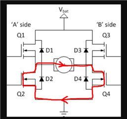
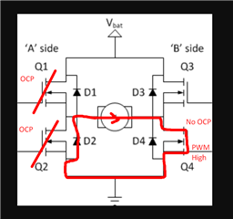
- We think this might be related to the slow decay, but we would need some support to verify that. Any other clues to find out the cause of our issue is also welcome.

- Performing the same test with a PWM of 20%, the current reach a value of 6A, but does not cause the driver to fail. Eventually the driver will enter in error due to over-temperature (we have a thermal camera measurement that confirms this). So our issue seems to be related to the high current consumption.

I remain available if you need additional information describing our issue,

Thank you for your responses!

  • Hi Antoine, 

    Thank you for reaching out to us. Would you provide us with the following request to better assist you. 

    1- Would you please share the whole schematic of DRV to be reviewed by us as well. 

    2- Would you please share the input as well. 

    3- The Input voltage is 48V, however, the output voltage seems to be higher than 48, which looks it is around 52 V.  Would you please make it clear?

    4- Have you captured the nFAULT and nSLeep during your test?


    Best regards, 

    Mojtaba

  • 1. Here is the entire schematic of the driver.

    As you might notice, the motor direction is managed by the signal "CAM_DIR" which could abruptly change the value of the PWM from PWM_INA to PWM_INB . At the control level, we ensure that there is no inversion of this signal with the PWM enabled. There is always a dead time of minimum 10ms between a change in direction with the PWM with a duty of 0. Our stall test does not involve direction change at the moment of break.

    2. Unfortunately I failed to get the inputs in a picoscope trace, and currently I don't have any hardware available to break.

    - We are confident that it is not the PWM that is at fault since our trace shows that the inverted voltage on the motor does not occur at a specific timing with respect to the PWM rising and falling edge.

    - We are confident that it is not the CAM_DIR signal as well. Our control resets the CAM_DIR to a default level when a fault is detected by the CAM, so this might be an issue, but we observed the failure in both direction of the motor, so there is no reason to think that this might have an impact in this issue.

    3. The input voltage is controlled by a LiFePo4 battery with connected charger (the failure also occurs without charger). In this test, the exact battery voltage is  52.4V.

    You made a good observation, during control, the PWM voltage reach ~51V. When the voltage is inverted in the above picture, the voltage reach ~56.21V, so higher that our battery voltage. At the time of inversion, the current was of 8.6A, knowing that, we should be able to understand a bit more about what happens during the failure.

    4. I did not capture the nFault / nSleep during my test.

  • Hi Antoine, 

    Thank you for sharing the information. 

    The schematic looks good, except the reason of using series resistors with the INx, ENx inputs. The inputs are internally pull down. The rest looks fine. As the information on your test bench is limited and there is no chance to collect more data, let me investigate it more internally and get back to you. I keep this thread open for the updates. 

  • Hello,

    My electronician was able to give me a new driver setup ^^ I reproduced the issue withtout the charger connected, so the voltage is sligtly lower (~47V battery voltage, and ~50V after inversion). This time my driver did not burn, but I think I was lucky since during the ~7 previous experiments it burned consistently. Maybe our problem is a limit case and the lower battery voltage could have saved us.

    I successfully got our inputs signals (CAM_PWM in brown, and CAM_DIR in green) when the over-current occurs. As we can see, our inputs signals are keeping the same logic since the fault is not detected by the software yet (The PWM keep the same duty / frequency, and the direction is the same). And the electrical signal itself seems to be quite clean, no interference are observed.

    However we observe an inversion of the output voltage level (red) that happens really quickly just like during the failure described in the previous post. After this event, the current will decrease up to 0. Once the current reach 0A, the inverted PWM disapear (the second frame illustrates the last measurement I have before the current reach 0, after that my trigger did not catch any positive output PWM).

    My current observations lead me to the idea that there is something strange happening when the overcurrent is triggered. We hope that you will be able to give us more information about this failure and what we could do to prevent the driver from burning in the future.

    I hope this helps you

    Antoine

  • Here is a bit more information about previous test with other measurements closer to the driver.

    brown signal: difference between PWM_INA and PWM_INB (so this excludes a potential fault from the pwm select chips)
    green signal: CAM_nFault --> proof that the driver enters in fault just at this time.

  • Hello again,

    I was still able to regenerate some interesting results, so I am sharing it with you to help you understanding our issue.

    This first image shows the result of an over-temperature. The difference from the over-current is that the voltage after the  fault (green signal) is a constant 50V instead of a PWM as we could observe previously for the over-current.

    We notice also that the nFault signal is quite noisy. This is due to the fact that the battery charger is connected. We believe it does not have any impact on the quality of the other signals.

    This second image shows the failure of the driver (so this is our last test...). We also notice that the inputs signals behave strangely after the fault. We believe that this is the consequence of the driver burning (and not the other way around).

    When investigating the datasheet, we noted a difference between the OCP and TSD. Our problem occurs only during Over-Current. Do you believe that it could be caused by the fact that we are driving the output in parallel in order to increase the drive current ? And that only one of the channel would enter in OCP, causing all the remaining current to flow by a single channel and eventually causing the driver to burn ?

    Best regards,

    Antoine

  • Hi Antonie, 

    I was still able to regenerate some interesting results, so I am sharing it with you to help you understanding our issue.

    This first image shows the result of an over-temperature. The difference from the over-current is that the voltage after the  fault (green signal) is a constant 50V instead of a PWM as we could observe previously for the over-current.

    We notice also that the nFault signal is quite noisy. This is due to the fact that the battery charger is connected. We believe it does not have any impact on the quality of the other signals

    As you mentioned correctly due to the temperature shutdown protection the FETs are disabled and as it is shown the VOUT goes to zero. However, I'm not sure why the output constantly fixed at 50V and then goes to zero. I think initially the OCP happened and then TSD. 

    As the temperature rise is one of the issues, would you please share the PCB layout with us? and Also please explain more about the stall condition and how you do it and when you release the motor to run. 

    Thank you

    Mojtaba

  • Hi Antonie, 

    Thank you for providing more information. 

    I successfully got our inputs signals (CAM_PWM in brown, and CAM_DIR in green) when the over-current occurs. As we can see, our inputs signals are keeping the same logic since the fault is not detected by the software yet (The PWM keep the same duty / frequency, and the direction is the same)

    As you connected the output in parallel mode, the current is splitting between outputs and increase the OCP threshold to 10 A or 5A for each FET. As shown below each channel has its own OCP and if the current in each FET is passing Iocp, that FET will be disabled. So, It is expected to DRV continue to work without any changes. Would you please explain more about the exact time the voltage is getting reversed. How do you stall the motor and when the motor continues running without stall. is it exact at the time the voltage is inversed? 

    However we observe an inversion of the output voltage level (red) that happens really quickly just like during the failure described in the previous post. After this event, the current will decrease up to 0. Once the current reach 0A, the inverted PWM disapear (the second frame illustrates the last measurement I have before the current reach 0, after that my trigger did not catch any positive output PWM).

    Would you please make it clear how did you measure the VOUT. From beginning, the CAMDIR is low and therefore the PWMINB is connected to GND and PWMINA is connected to the CAMPWM. It is expected that the output voltage is varying between VM and GND, however in your case it is experiencing negative voltage. would you please let me know how it is measured?

  • Hi Antonie, 

    it seems that the nFAULT is due to OCP and as mentioned in the datasheet the channel experiencing the overcurrent will be disabled. It seems that the current is not splitting equally to the FETs and one of them is experiencing overcurrent which can detect minimum 3A OCP.

    I'm wondering if the paths for outs are experiencing different inductance and resistance which lead to not splitting equally. Would you please share the PCB layout with us to be reviewed.

  • Hello

    Our motor is connected through a wormgear to a cam (similar to the below illustration found on the internet). When reversing the motion, the cam stalls against the follower. During my latest test, the stall test was successfull many times (OCP correctly triggered and the driver could continue its operation afterwards). The driver only broke when I started the motion with the cam already stalled. In this case the current rise happens much more quickly and the driver broke.

    ---

    The VOUT is measured by connecting a differential probe to the driver output. 1 end connected to the (OUT1/OUT2), 1 end connected to the (OUT3/OUT4). I connected the probes without paying attention to the direction since I only needed the DeltaV.

    As I understand it, the output voltage will be a positive PWM for forward motion of the motor, and a negative PWM for reverse motion of the motor. This means that during this test the motor was in reverse direction. Note that the problem occurs in both direction of the motor.

  • I'm wondering if the paths for outs are experiencing different inductance and resistance which lead to not splitting equally. Would you please share the PCB layout with us to be reviewed.

    Hi Motjaba,

    I am the HW designer of the board.

    Here is a capture of each layer of the layout around the driver: L1=RED, L2=GREEN, L3=BROWN, L4=BLUE.

    L2 (GND plane)

    L3 (GND plane below the driver)

    L4

    Moreover, to increase heat dissipation from bottom plane, we removed the soldermask locally on bottom side under the chip (see flipped view compared to 2D layer views):

    As you can see on L1, the parallelization of OUT1/OUT2 and OUT3/OUT4 is direct at the output of the driver, so each pair of channel should not see much inductance and resistance difference.

    Sorry, I am not actively participating to this investigation as I am busy on other projects but I hope this will help.

  • However, I'm not sure why the output constantly fixed at 50V and then goes to zero. I think initially the OCP happened and then TSD. 

    In my opinion, the "negative" voltage is the motor's regeneration voltage. It is fixed to 50V due to the body diode of the FETs clamping the motor voltage to Vbat+2*Vsd (more on that below).

    PWM-High before nFault:

    PWM-Low before nFault: the motor coil tends to maintain current in the same direction but its voltage is shorted by Q2 and Q4 

    When OCP/TSD occurs (PWM-still low): all FETs are open, current is maintained by motor coil, hence voltage is inverted from motor pov. The current finds its path through D2 and D3

    In this case Vbat=-Vd2+Vmot-Vd3 <=> Vmot = Vbat + Vd2 + Vd3 <=> Vmot > Vbat

    As Vbat, Vd2 and Vd3 are assumed constant during this period, the voltage is clamped a little bit above the battery voltage.

    Now real question is: why the PWM has an impact on the motor voltage when OCP occurs ?

    By writing this answer, I think I got the anwer: our measurements tend to show that Q1 is still driven by the PWM when OCP occurs on Q2 and/or Q4. We can only assume that Q1 has no OCP triggered (because it trigs during regeneration (fig 2 -> Q2 and Q4 involved)). But should it be ? Why OCP does not disable the pair of FETs (Q1 & Q4)?

    The PWM is meant to drive Q1 and Q4 pair, as on the first picture because we did not change the PWM input. If then Q1 is enabled (because no OCP), Vmot is shorted at e.g. 30% duty cycle (instead of supplying current through Q1-Q4 30% of the time) which gives the impression (from Vmot pov) to apply a 70% duty cycle. 

    If this is correct, the failure happens when Q1 is closing but I am not sure as of why? Why OCP of Q1 does not trigger anyway? Ideas are welcome about that :)

    So our issue seems to be related to the high current consumption.

    While in TSD, all FET are well disabled and the situation is maintained until the motor has returned all its energy.

    Conclusion

    So I think we got our answer to apply in the current system.

    --> We should definitely cut the PWM instantly (by HW - safe by design) when a Fault is detected.

    Also this could bring a conclusion for TI chip designer that, we might want to have TSD behaviour (i.e. cut the drive of all FETs in the chip or at least of the FET's pair concerned with OCP) whenever a Fault is triggered. The OCP description is not very detailed in the datasheet and it is hard to anticipate such failure behaviour. I don't know if there are use cases where cutting individual FET is useful (I can imagine that if the driver is not used as an H-Bridge but that's not the main purpose of the chip).

    Also, we miss an explaination about why Q1 (in the given example) does still react to the PWM despite OCP on the other FET of its pair (Q4) and why OCP does not trig when the overcurrent happens on Q1 after the fault.

    Thank you for your help !

    Best regards,

  • Hi Antonie, 

    Thank you for your information. 

    The PCB layout looks fine, and all consideration has been followed by the designer. 

    Now real question is: why the PWM has an impact on the motor voltage when OCP occurs ?

    By writing this answer, I think I got the anwer: our measurements tend to show that Q1 is still driven by the PWM when OCP occurs on Q2 and/or Q4. We can only assume that Q1 has no OCP triggered (because it trigs during regeneration (fig 2 -> Q2 and Q4 involved)). But should it be ? Why OCP does not disable the pair of FETs (Q1 & Q4)?

    As shown each FET has an analog current circuit which measure the current for OCP detection. In parallel mode the OCP level will be increase to 2XIOCP as the output current is splitting between the channels. The IOCP min is 3 A and typical is 5A. and this value can different for each channel. so in parralel mode, one of the channels may detect the OCP and at the same time the other is still working properly. This issue may result in some situations in which the output voltage is still active even the OCP is detected by one of the channels. 

    The figure below, shows that the DRV will be disabled due to temperature shutdown and this conditions will disable all FETs.  In the scenario below the current on each FET is 2.4 A and it results in 4 (FETs)x0.24 (ohm) x2.4^2 (A)x31.6(C/W) = 174C which is higher than Thermal shutdown temperature 160 C and therefore TSD disable all FETs.  

    Under the following circumstances, the output voltage is still available even if the nFAULT goes low.  


    To explain the condition above, let's consider the motor is operating in FWD direction and current is passing through Q1 and Q4. the voltage Vm is across the motor. and the Vout is changing between 0 to Vm. 

    When nFAULT happens the BH and BL detect OCP and will be disabled. So to let the current flowing, the AL and body diode of BH pass the current and let the motor to operate under fast decay mode as shown below.. This Fast decay mode put -VM on the motor wqindings. Therefore  the motor current is decreasing to zero. and as you noted 

    After this event, the current will decrease up to 0. Once the current reach 0A, the inverted PWM disapear (the second frame illustrates the last measurement I have before the current reach 0, after that my trigger did not catch any positive output PWM

    after reaching to zero amps, the PWM cannot trigger any FETs  as BH and BL are disabled due to OCP and they will remain off until either RESET is asserted or VM power is cycled"

    The Over current protection only disable the channel that exposed to OCP, and let the other channel continue working. If due to parallel mode only one of the channels detect OCP and being disabled, the other one can operate the motor under the fast decay mode and let output voltage continuously apply to the motor. Therefore, unlike the single channel operation that OCP detection disable the output completely, under parallel mode OCP may only disable one channel and as the channels are paralleled the other one will provide the path for the current. 

    The  RDSon difference between channels lead to experiencing different IOCP threshold and one of them may be disabled and the other one still work. This issue is not happening in single channel because each channel separately detects OCP and disable itself. So no inference happens between channels. 

    Under Temperature shut down, we do not face this issue, because when it happens, all FETs are being disabled. 

    So I think we got our answer to apply in the current system.

    --> We should definitely cut the PWM instantly (by HW - safe by design) when a Fault is detected.

    Also this could bring a conclusion for TI chip designer that, we might want to have TSD behaviour (i.e. cut the drive of all FETs in the chip or at least of the FET's pair concerned with OCP) whenever a Fault is triggered. The OCP description is not very detailed in the datasheet and it is hard to anticipate such failure behaviour. I don't know if there are use cases where cutting individual FET is useful (I can imagine that if the driver is not used as an H-Bridge but that's not the main purpose of the chip).

    Also, we miss an explaination about why Q1 (in the given example) does still react to the PWM despite OCP on the other FET of its pair (Q4) and why OCP does not trig when the overcurrent happens on Q1 after the fault.

    As already explained the condition when the fault is happening, under parallel mode you should cut the PWM when a fault is happening, because OCP only disable the channel experiencing overcurrent and maybe only one of the channels detects the over current and this condition results in reverse voltage on the outputs. In the case of high current, and also charging, this reverse voltage may expose high stress on the DRV and damage it. 

    To prevent the failure issue, as you also concluded, it is better to cut the PWM when a fault detected by the DRV and stop the DRV to operate under undefined conditions.  

    Moreover, please consider that the maximum continuous output current is 2.5A for each channel and any current beyond it may cause permanent damage to the device

    Please let me know if  you have any questions. 

    Best regards, 

    Mojtaba.

  • Hello Mojtaba,

    Thank you for your support and highlighting that a channel disabled by OCP is either the branch AH/AL or BH/BL.

    I'll correct hereunder the reasoning (conclusion remains unchanged)

    PWM-High before nFault:

    PWM-Low before nFault: the motor coil tends to maintain current in the same direction but its voltage is shorted by Q2 and Q4 

    When OCP/TSD occurs (PWM-still low): all FETs are open, current is maintained by motor coil, hence voltage is inverted from motor pov. The current finds its path through D2 and D3

    [UPDATED PIC]

    SCENARIO A:

    PWM low when OCP occurs:


    When PWM goes high again:

    We also have a second possibility as the current in fig 2 can trigger either channel (Q1/Q2 or Q3/Q4) that has the lower IOCP.

    SCENARIO B:

    PWM low when OCP occurs:

    When PWM goes high again:

    --> Current paths are different but from motor voltage point of view it is the same: the motor voltage is shorted when PWM is high (on the channel without OCP) and regenerating when PWM low. 

    --> Now considering that both paralleled channel could have their OCP on scenario A and B, we could have one channel doing this:

    While the other doing this:

    And now the motor goes from regeneration (-48V) to being supplied (+48V) with Q1-A and Q4-B that is equivalent to only one channel instead of 2 in parallel but carrying the high current that was meant for 2.

    Now, regarding your explaination here:

    under parallel mode you should cut the PWM when a fault is happening, because OCP only disable the channel experiencing overcurrent and maybe only one of the channels detects the over current and this condition results in reverse voltage on the outputs.

    I understand what you convey but in that case I have 2 remarks:

    1. When the first (of the two paralleled) channel is experiencing OCP, that channels is disabled. As we measured we have more than 7A. Those amps do not disappear when the first channel trigs the OCP as the motor coils tend to give inertia to the current. Therefore, all of those 7A (>>5A typical) immediately start flowing in the second channel that most certainly also triggers OCP. That's why I only considered one channel in my development; I assume that if one channel trigs OCP, right after, the second one should also trig OCP as it receives the current that was shared with 2 channels.

    --> Do you mean that if one channel trigs OCP, the other channels cannot trig OCP anymore ?

    2. If we assume that only one channel trigs OCP and the paralleled one does not, the first channel is simply disabled and should not interfere with the second that is still working. Hence, we should not see a reverse voltage on the output but simply the normal operation as it's only Channel 2 that is dictating the motor voltage (as long as Channel 2 holds up of course...).