This thread has been locked.

If you have a related question, please click the "Ask a related question" button in the top right corner. The newly created question will be automatically linked to this question.

DRV2700: Flyback maximum duty cycle

Part Number: DRV2700

Tool/software:

Hi there,

I am currently troubleshooting a custom implementation of DRV2700 based on DRV2700EVM-HV500. My design is implemented almost exactly as per the reference design, aside from a few key differences:

  • I am using a custom wound flyback transformer based on ETD29 core with 0.9 mm gap. The primary winding is 15 turns, and the secondary is formed from 4 x 93 turn windings, wired in series, for a total input:output turns ratio of 1:25.
    • Each secondary winding has an S8CMHQ flyback diode and 10 nF 3 kV ceramic capacitor.
    • I've measured the primary inductance at 19.5 uH
  • I am using a higher voltage rated MOSFET than the EVM - IXTA02N250HV.
  • My feedback resistors are: 20 MegOhm, 1 kOhm and 10 kOhm.
  • My lower feedback resistor is driven by an opamp betwenn 0 and 1.3 V to adjust the HV output between 0 and ~2 kV.

When I try and drive the output voltage beyond 1 kV, I find that the voltage on the FB pin sags, and the output voltage no longer increases. I noticed that when probing the switch pin with the PWM duty cycle set beyond ~ 55 (beyond the duty point that causes V_FB to sag), the DRV2700 appears to be driving the controller at around 90 % duty cycle. Have I reached the limitations of what the IC can do here?

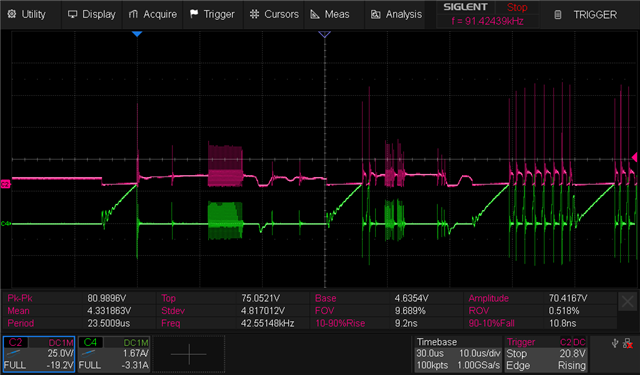
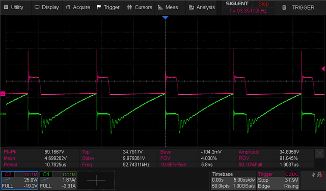
The first two screenshots are with my PWM duty configured such that an output voltage of 650 V is developed. The converter is operating in a mode where a burst of pulses appear at the SW node (channel 3). The output voltage is shown on channel 1. The second screenshot is a close up of the switching event.The duty cycle is around 90 %.

The next two screenshots are when I increase the PWM duty beyond 55 (50 in this case), which is at the point where the output voltage no longer increases, and the FB pin voltage sags. The output voltage is much steadier, at around 1 kV, and the SW node looks very similar. The difference with this mode is that there is no pulse skipping, the SW node is constantly switching at around 90 % duty:

Currently the output is loaded with around 13 MOhms of resistance, plus a MICSIG isolated differential oscilloscope probe DP3002 (rated for 3 kV). There is also 10 nF of bypass capacitance, at the output. The REXT value is set at 6 kOhm (the minimum recommended value). 

Thanks in advance for your help.

  • Hi Toby,

    Thanks for reaching out. It sounds like you have a great grasp on the flyback converter here!

    The one thing that caught my attention was the feedback resistor values - your sum total is >20Mohm. Our user guide recommends 500k-1M, so I wonder if reducing those values makes a difference. 

    DRV2700 appears to be driving the controller at around 90 % duty cycle. Have I reached the limitations of what the IC can do here?

    I was digging into our old validation data to see if there is some data around this, but I was not able to find anything. I will check to see if there is any other resource to help here. 

  • Hi Kelly,

    Thank you for your suggestion. I tried reducing my feedback network from 20 Meg, 10 k, and 1 k, to 1 Meg, 510 R and 51 R. This made no difference to the behaviour.

    I have captured some waveforms at the SW node, as well as the voltage across a 0.12 Ohm shunt that is in between the SW node and the primary winding.

    The first screenshot shows the behaviour straight from startup. The second screenshot is after a few seconds of operation. I notice also that my SW node peaks at around 117 V. This is evidently being caught by the Schottky + Zener snubber I used, however this is beyond the maximum ratings of the FET. I will try a lower voltage Zener, in case I am damaging the primary FET and affecting the operation of the device.

  • Hi,

    Just a quick update with some further testing I've done.

    The above 2 screenshots in my last reply were actually captured using a newly wound flyback transformer. I was concerned that primary to secondary capacitance was too high, so I wound another with the primary separate on one side of the bobbin, and the secondaries on the other side. This however greatly increased the leakage inductance, which I believed caused excessive heating in the diode snubber network. I've now returned to a stacked winding approach, with the primary closest to the core and secondaries on top. I have 12 turns of primary and 4 x 72 turns of secondary. I now get the following waveforms, but still experience feedback voltage sag if I try and push the output voltage too far:

    Startup:

    Continuous run with voltage limiting:

  • Hi,

    I managed to get the design working up to 2 kV this afternoon. I replaced the S8CMHQ output diodes with the part used in DRV2700EVM-HV500 (4 of MMBD3004S-7-F in series per output winding). I am not entirely sure why this worked, but I do have a theory:

    S8CMHQ has around 70 pF of capacitance, whereas the series string of MMBD3004S-7-Fs I replaced it with should be under 1 pF per winding. I think it is possible that the 70 pF of diode capacitance was ringing in combination with the leakage inductance on the secondary side of my flyback transformer. Looking trough the datasheets for the two parts, I can't really see any other major differences.

    I'd be keen to hear if anyone else has thoughts on what might have happened here.

  • Hi Toby,

    It is great to hear you were able to resolve the issue here. I hope it is sufficient to continue moving forward.

    I was looking into it the other day and not really able to understand how to improve the system - this is a little bit outside of the typical use cases we see of DRV2700. We don't have an expert on Flyback converters on the team at this point in time (they left in ~2018). I reached out to some colleagues but haven't received a response yet.