This thread has been locked.

If you have a related question, please click the "Ask a related question" button in the top right corner. The newly created question will be automatically linked to this question.

DRV8870: DRV8870DDA SO8 - last PCN

Part Number: DRV8870
Other Parts Discussed in Thread: DRV8251

Tool/software:

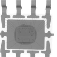
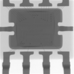
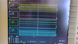
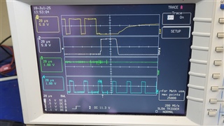
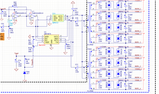
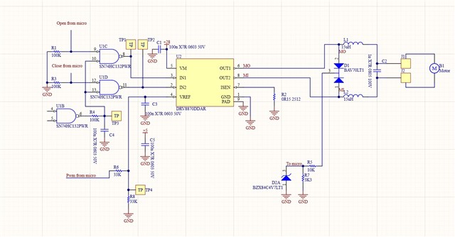
We notice different x-ray ouput before (ligher) and after (darker) the PCN having effective date FEb-2024, pn DRV8870DDA.

We red that fit form and function didn't changed but at the end of the day the device is not working; for every PCBA we have to replace the device with and the version before the last PCN release.
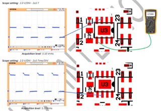
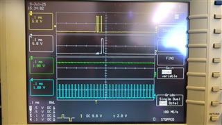
Any suggestions?

  • Hello Alberto,

    Thanks for your question.

    Could you please help understand the issue on DRV8870? Any waveforms or schematic diagrams to understand the failure would be helpful.

    Thanks,

    Ibinu

  • The problem is only on the outputs, power and input signals are regular even on the post PCN drivers.

  • Thanks Alberto for confirming. Let me work with the team and get back to you

  • Hi Alberto, 

    Thank you for providing information. 

    Would you please provide me more information about the issue that customer is facing with new devices compared to old devices. Would you please provide me with the outputs from old devices as well and explain the issue. 

    Best regards, 
    Mojtaba.

  • The VM power supply values ​​and logic signals at the inputs are aligned with the standard operating parameters observed with pre-PCN devices, but we have complete absence of driver output signal.
  • Hi Alberto, 

    Thank you for your reply. 

    To be confirmed, For the post-PCN devices, there is no output with applying appropriate input.?

    In this case, 

    would you please confirm that you have seen this issue for all post PCN  devices?

    Would you please share your schematic with us?

    The problem is only on the outputs, power and input signals are regular even on the post PCN drivers.

    Is the shared waveform for pre-PCN deveices?

    Best regards, 

    Mojtaba.

  • I have the same problem. I have a lot of 1000 boards with new version and all are not working. All board works if I change the driver with the old one. The image shows scope screen with driver outputs top and driver inputs bottom. The expected behavior is an output always low and the other output with PWM.

    .

  • Hi Riccardo, 

    Thank you for the information. 

    Would you please let us know what the application is, and also would it be possible to share the schematic for the DRV8870 with me. 

    Best regards,

    Mojtaba.

  • Hi Alberto and Riccardo,

    It's not clear from your scope capture which output signals are from which device. If possible, please provide scope capture of both input signals (IN1 and IN2) and both output signals (OUT1 and OUT2). Providing these will allow us to understand between which current recirculation is being used during PWM off time. From the captures provided it's not clear whether the switching sequence is between FWD/COAST or FWD/BRAKE state. 

    There are no spec changes between devices that had PCN, therefore it seems strange that the boards are "not working". By providing the schematics and layouts we could help to debug further.

    Are there any thresholds that disable outputs at a certain state or condition?

    If the outputs are Hi-Z is there any external circuitry that could be affected?

    Best,

    David

  • I have replaced DRV8870 with DRV8251 and it works.:

    The image shows the signals. As the previous image, the signals are:

    Channel 1 OUT2

    Channel 2 OUT1

    Channel 3 IN2

    Channel 4 IN1

    The switching sequence is between FWD/BRAKE

    The threshold is higher than the current.

    We have already produced more than 20000 boards without problems.

  • Unfortunately, even the DRV8251 is not working properly. 

    It seems more sensible to the noise of the motor’s brushes commutation.

  • From our side, we are modifying some components: we have this schematics

    we tried with

    R97 = NM → Vref = 4.7 V
    R98 = 330 mΩ
    Cx066 and Cx068 = 100 nF, to reduce the charging time.

    We also observed that the DRV starts operating at 6.5 V, so delaying Vmid with Soft Start is pointless.
    There is no benefit in acting on the SYNC_F synchronization signal, since it triggers well before the DRV.

    Results obtained:

    • The amplifier stage is back to working properly.

    • GATE voltage with MOSFET ON = 12.3 V, compared to 12.9 V without the modification.

    BUT at the end of the day the TEST was KO

    It is unbelievable that TI changed so much with this declared PCN  !!!!! PLEASE ONE OF TI TECH TECH EXPLAIN!

  • Hi Alberto, 

    Thank you for the update. Let me check the inforamtion and get back to you by EOD. 

    Best regards,

    Mojtaba

  • Hi Alberto, 

    Thank you for the information. Sorry for late reply, the e2e was down on Friday. 

    I have reviewed the schematic. I have some questions regarding the schematic. 

    R97 = NM → Vref = 4.7 V
    R98 = 330 mΩ

    connecting ISEN to GND through Rsense resistor enable the current regulation and regulate the current at ITRIP (A). in the current schematic ISEN is connected to GND through a 50 m ohm res which leads to  ITRIP = 4.7 / (10 *  0.05) = 9.4 A which is not a correct value for Itirp since the driver can devliver up 3.6A peak current. For modified R98 = 0.33 ohm the ITRIP is = 4.7/ (10*0.33) = 1.42 A which allow the current regulation work properly. 

    We also observed that the DRV starts operating at 6.5 V, so delaying Vmid with Soft Start is pointless.
    There is no benefit in acting on the SYNC_F synchronization signal, since it triggers well before the DRV.

    The DRV8870 operating voltage is 6.5 V to 45 V.  We have not tested DRV8870 with MP6613 driver.  Would you please let me know what is the reason behind using the delaying Vmid?

    Results obtained:

    • The amplifier stage is back to working properly.

    • GATE voltage with MOSFET ON = 12.3 V, compared to 12.9 V without the modification.

    Would you please explain what you mean by GATE voltage? The DRV8870 has integrated FET and the output is changing between 0 and VM value.

    Best regards, 

    Mojtaba.

  • Do you have suggestions about my application?

    My application is a typical brushed DC motor driven in PWM.

    Everything was designed following the prescriptions in the datasheet.

    It has worked well on more than 20000 products in the last 6 years.

    It has worked well attached to 4 different motors.

    Now production is on hold waiting for a solution.

    It seems that some protection is triggered by the spikes generated by the motor.

    Can you identify which protection is triggered?

    How can I protect it?

  • After some other tests, I think the problem is in OCP. I can say that because the driver retries to start after 3ms, equal to tRETRY.

    I find peaks of current when the motor is rotating of about 20 A but they are 20-30ns long.

    They should not trigger the OCP because tOCP is 1.5us and shorter impulse should be filtered.

    The other problem is that it doesn’t restart after 3ms and there isn’t any overcurrent fault.

    .

  • Hi Riccardo, 

    Thank you for the update. 

    I'm investigating about this issue with the design team and get back to you with the update. In the meantime, would you please provide me with the following information. 

    After some other tests, I think the problem is in OCP. I can say that because the driver retries to start after 3ms, equal to tRETRY.

    I find peaks of current when the motor is rotating of about 20 A but they are 20-30ns long.

    They should not trigger the OCP because tOCP is 1.5us and shorter impulse should be filtered

     The DRV8870 typical IOCP is 4.5 A with deglitch time of 1.5 us. The Hbridge are disabled for a 3ms and then reenable the outputs. 

    However MP6513 has 2A IOCP with 0.85 ms retry time. these differences may cause some interferences. 

    What is the steady state current of the motor? what is the DRV input voltage? What is the PWM frequency?

    Would you please share a capture of current waveform, and outputs?

    The other problem is that it doesn’t restart after 3ms and there isn’t any overcurrent fault.

    If the overcurrent fault is still present, the cycle repeats, otherwise normal device operation resumes.

    R97 = NM → Vref = 4.7 V
    R98 = 330 mΩ
    Cx066 and Cx068 = 100 nF, to reduce the charging time.

    We also observed that the DRV starts operating at 6.5 V, so delaying Vmid with Soft Start is pointless.
    There is no benefit in acting on the SYNC_F synchronization signal, since it triggers well before the DRV.

    Results obtained:

    • The amplifier stage is back to working properly.

    • GATE voltage with MOSFET ON = 12.3 V, compared to 12.9 V without the modification.

    Changing R98 to 330 mohm enables the current regulation and limit the currents to 4.7/ (10*0.33) = 1.42 A. is the board working fine after this change? 

    This modification led to limiting the BDC inrush current and prevent the OCP triggering due to inrush current. 

    Best regards, 

    Mojtaba

  • Don't make confusion. I'm talking about my project which is different to the project of Alberto


    .

    My project is a simple driver for dc brushed motor.

    All my comments refers to my project.

    Maybe we should open another topic because the circuit of Alberto is much different.

  • Hi Ricardo, 

    Yes, please post your issue into a new thread. 

    Best regards, 

    Mojtaba 

  • Hi Alberto, 

    Does changing R98 solve the issue? Please let us know if you still have issue with the driver.  

    Best regards, 

    Mojtaba

  • Hi Ricardo, 

    Thank you for posting your question. We will follow up with you on new thread.

    Best regards, 

    Mojtaba