This thread has been locked.

If you have a related question, please click the "Ask a related question" button in the top right corner. The newly created question will be automatically linked to this question.

DRV8353F: Dead time / Overcurrent / Layout

Part Number: DRV8353F
Other Parts Discussed in Thread: DRV8353

Tool/software:

Hi All


I have a question about DRV8353F.


(1) As stated in the document Understanding Smart Gate Drive, will the dead time change because the dead time is optimized?
     https://www.ti.com/jp/lit/an/slva714d/slva714d.pdf


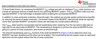
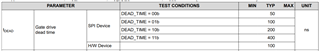
    Or is it fixed at the standard value described in the specs below?


(2) It is stated that the operation when SPI is overcurrent operates in cycle-by-cycle (CBC) mode by default, but does this mean the same as Automatic Retry in OCP_MODE?

(3) We are considering both the DRV8353F (40 pin) and the DRV8353 (40 pin), and plan to use a common layout.
     The DRV8353 data sheet does not include a reference layout for the 40 pin. Is it okay to use the same layout as the DRV8353F data sheet?


Best Regards,
Ishiwata

  • Hello,

    1. The dead time will be fixed at the value you set to in the spec table.

    2. The device operates with CBC active only when OCP_MODE = 01b. By default, the device will retry EITHER when new rising edge on PWM input is given (CBC) OR after T(retry) time passes.

    If you want to have only T(retry) and no CBC fault clear, you can change the bit shown below to 0b

    3. Yes, they can share common layout as they share the same pinout

    Thank you,

    Joseph

  • Hello Joseph,


    Thank you for your answer.


    I have an additional question.

    (2) About overcurrent
      I still don't understand the difference between CBC 0b and 1b.
      Are there any waveforms that show the operation? Do both operate intermittently due to auto-retry operation?
      In the case of operate intermittently, does the current transition like a limited current around the OCP threshold?

    (3) About layout
      I have a question about GND and AGND.
      In the reference layout, GND and AGND are connected on the same layer.


      Can GND and AGND be shared? Or is it better to separate them?
      When I checked the data sheet, it says to connect to AGND.


      I'm not sure whether I need to separate GND and AGND.


    Best Regards,
    Ishiwata

  • Hi Ishiwata,

    (2). CBC mode is only able to be set to 1b if OCP_MODE is already set to auto-retry.

    When CBC is 0b, Device clear fault condition and retry ONLY after T(retry) has passed.

    When CBC is 1b, Device clears fault condition either after device receives new rising edge on INHx or INLx, or after T(retry) has passed.

    CBC = 1b can give you a faster retry, since you won't have to wait for T(retry) to pass in order for device to attempt to recover automatically.

    (3). AGND and GND should be seperate, AGND is for quiet analog signals, where GND is for the noisier power GND. AGND is seperate in order to protect the sensitive signals like CSA output to MCU from noise from power stage GND. You can see this picture below for more detail.

    Thank you,

    Joseph

  • Hello Joseph,

    Thank you for your answer.

    (2) Regarding overcurrent operation,
    I will check your answer.

    (3) Regarding the layout
    In the 11.2 Layout Example, GND and AGND are the same. This seems different from your answer, so which one is correct?

    Best Regards,
    Ishiwata

  • Hi Ishiwata,

    (3)

    Either method can be used.

    You can see in the Layout Example 11.2, the MCU signals are kept away from the power/switching signals to avoid noise propagation. You can connect AGND and GND on the same plane like shown in the layout example, just make sure to separate the sensitive signals from noisy switching signals. 

    Thank you,

    Joseph