This thread has been locked.

If you have a related question, please click the "Ask a related question" button in the top right corner. The newly created question will be automatically linked to this question.

DRV8412: The DRV8412 is Protection is prone to occur.

Part Number: DRV8412

Tool/software:

Dear

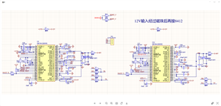
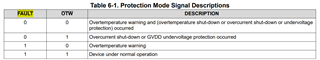
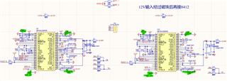
   MP: When using the 8412 parallel drive output and increasing the drive current solution, the peak-to-peak output current of the chip is 7A. The IC is prone to protection. What is the reason for this? 

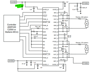
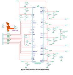
The current configuration resistance is 27K,  Two chips are connected in parallel with three half-bridge outputs to drive a three-phase stepping motor.

  • Hi liu, 

    Thank you for your question. 

    When using the 8412 parallel drive output and increasing the drive current solution, the peak-to-peak output current of the chip is 7A.

    This device can deliver continuous output current up to 3A per Hbridge or 6A per full bridge. In your case, 7A is higher than the maximum current. However, the OCP is set to 9.7 A but would you please check the nFAULT , OTW pins to see 1- Which protection is enabled and 2- which device is prone to fault. 

    Please update me with the capture of FAUlt and OTW pins when device is prone to protection. 

    Best regards, 

    Mojtaba.

  • Hi  Mojtaba

        thank you  ,  Now, even when I'm not connected to a motor, I still have a drive protection (this drive is connected to two phases of a three-phase motor), with only the FAULT pin being 0 and the OWT pin is 1 , 

    As long as there is a problem with this board, it will always be like this. Even repeated power-off and power-on operations won't work.

  • Hi Liu, 

    Thank you for the update. 

    Would you please 

    1- explain the which device is enabling the protection. 

    2- For Fault =0 , OTW = 1, we expect to have overcurrent protection shutdown, or GVDD under voltage protection. Please capture a screenshot of FAULT and OTW , GVDD pins and OUTA current. 

    3- TI recommends to use a bulk capacitor on GVDD pins (Highlighted below) to prevent any dip on GVDD voltage. Could you please confirm it on your design. 

    4-Is there a reason that you used different capacitors 1uF and 10uF on the GVDD pins. 

    5- How much is the L values on the output pin. Why did you use them?

    Best regards, 

    Mojtaba.