This thread has been locked.

If you have a related question, please click the "Ask a related question" button in the top right corner. The newly created question will be automatically linked to this question.

DRV8329: circuit was not working and nFAULT was asserted.

Part Number: DRV8329

Tool/software:

Hi expert,

My client is currently using DRV8329, when the circuit is powered on without load, the MCU provides a drive signal, but the device is unable to operate, and the nfault pin remains pulled low. After investigation, disabling the Vds overcurrent protection feature( by connecting VDSLVL to GVDD through a 100 kΩ resistor. ) allows the device to return to normal operation. 

After testing, the MOSFET turn-on time is about 500 ns, with the load current being 0. I would like to know

1. what causes the nfault pin to be pulled low constantly.

2. Currently, disabling the Vds overcurrent protection can allow the circuit to resume operation, but it loses overcurrent protection functionality. How can this be improved?

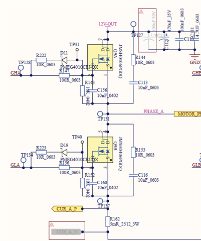
Below are some schematics:
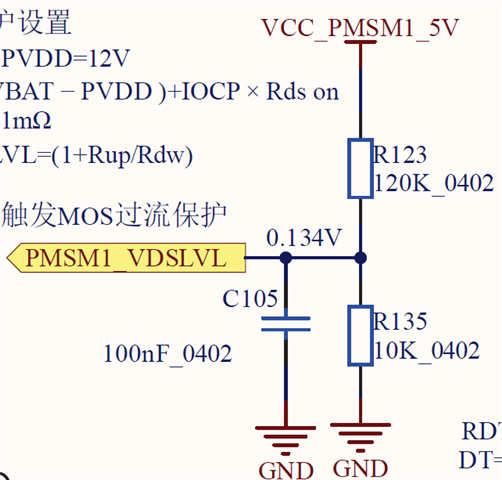
VDSLVL

drive circuit

  • Hello Longbiao,

    Thank you for the question. I will get back to you before the end of the week!

    Cheers,
    Joel A. A.

  • Dear Longbiao,


    Thank you for your patience! Here are my responses to the client's questions.


    Why their nFAULT pin remains pulled low?


    Typically, the nFAULT in this device starts low until certain waking parameters are met within a prescribed timeframe. Because there are several faults that can prevent the nFAULT from going high, I will need to see a scope with timings to narrow possible reasons for their issue.


    Why disabling VDS overcurrent protection allows the device to return to normal operation?

    For our DRV8329, disabling the VDS (and VSENSE) overcurrent protection by connecting VDSLVL to GVDD through a 100kilo-ohm resistor effectively raises the VDS overcurrent threshold (VDS_OCP) to around 4.2V.


    If their nFAULT is high (and allowing normal operation) in this state could mean one of the following:

    • That their base configuration, with a lower VDSLVL, trips VDS_OCP.
    • That their base configuration trips VSENSE, which has its threshold set at 0.5V, trips SEN_OCP.


    It would be useful to know what current they observe (vs expect) through their FETs. Also, could they clarify what they mean by the circuit is powered on 'without load'?


    Cheers,

    Joel A. Adejola