Tool/software:
Hi,
I've recently ordered a batch of BLDC drivers that I have designed around DRV8302. It is a third iteration of the same design (it has some minor changes in layout). So I have 2 fully working prototypes in the workshop. My problem is that the new drivers have their GVDD pin at 0V all the time, which results in nFault pin going low and no output being produced.
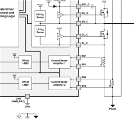
Only major thing that is different in the new driver is the current sense (both SP and SN 1/2). I removed the low-side current sensing setup and replaced it with inline one. Is this is a problem? Is the DRV8302 dependent on the low-side sensing setup presence?
I also tried to reduce distance between the large GND pad of the chip and source pins of the low side mosfets with wires, but I had no luck with that. DVDD and PVDD voltages are at expected levels. Specifically:
DVDD = 3.45V
PVDD1 = 20.0V (powered from 20V power supply)
But GVDD and AVDD are both at 0V.
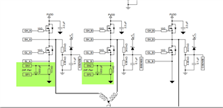
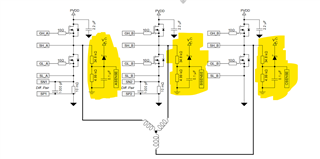
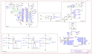
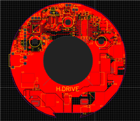
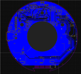
This is my schematic and layout:
Does anyone know what could be the cause?