Other Parts Discussed in Thread: DRV8323
Tool/software:
Hi,
I'm currently learning how to use the SPI communication of the DRV8323RS, but I've encountered some problems and I don't know how to solve them.
Firstly, the 3.3V output of DRV8323 is normal. The enable pin has been pulled high, and the nFault pin is also at a high level.My SPI host is configured as follows: clock phase is 1 (the second edge is captured), clock polarity is 0, and MSB data is sent first.
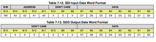
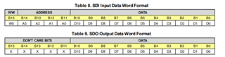
For example, if I want to check the default value of the CSA Control Register (with the address of 0x06), I need to send the value 0xB000 (1011 0000 0000 0000). Then, the value I will receive will be 0x0283 (0000 0010 1000 0011).If I send the write command first, setting each bit of the CSA Control Register to 1 and then reading the register, I need to send 0x37FF (0011 0111 1111 1111) first, followed by 0xB000. The value I will obtain will be 0x07FF.But in fact, I can only receive 0x0083. This means that the instructions I sent for writing were not executed, and the data received by the read instructions was incomplete.
Before this, I had used the SPI communication of DRV8703 without any problems. However, when I switched to DRV8323, there were issues. I wonder if I missed something.It would be great if someone could offer some ideas.
Best wishes,
huan yin