This thread has been locked.

If you have a related question, please click the "Ask a related question" button in the top right corner. The newly created question will be automatically linked to this question.

DRV8262: DRV8262

Part Number: DRV8262

Tool/software:

Hi again, 

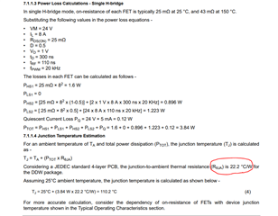
In DRV8262 datasheet, when power loss is calculated in the example below, it mentions that they use 22.2 C/W as Rja considering a JEDEC standard 4 layer PCB. 

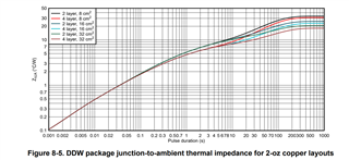
It seems that the example shown there is PWM signals. Why do they use DC parameter of Rja in this case? Shouldn't I look into thermal impedance plot over duty cycle? In the example, duty cycle is 0.5 and frequency is 20kHz, so looking at the thermal impedance plot at 0.025ms (0.05ms/2) gives me much lower Rja. I wanted to clarify why 22.2C/W is used instead. It seems that 22.2C/W is Rja at DC operation. 

  • Hi Jake,

    You are correct. The example shown was for 20 kHz PWM input with duty cycle D = 0.5 (50 %). This 50 % duty cycle was considered and compensated for while calculating the losses in each FET. It was only half the power vs. DC operation. Because of this calculation, the FET power loss was normalized for DC, and because of this reason 22.2 C/W was used for Rja. The switching losses happen only during rising and falling edges at the FET and does not change with duty cycle. 

    so looking at the thermal impedance plot at 0.025ms (0.05ms/2) gives me much lower Rja.

    Which thermal impedance plot you were referring to? 

    Regards, Murugavel 

  • Hello, 

    I am referring this plot in the datasheet. At 0.025ms, I am seeing Zja around 0.9 or 1. Unless this is different than what it is called thermal impedance plot for SOA of normal transistors? I still did not understand why 22.2C/W is used. For my case, it will use as single H-bridge but more DC operation (no PWM) for a certain period of time, let's say 20s max. Then I should refer to thermal impedance plot to find thermal resistance instead of using 22.2C/W, is this correct? I see thermal impedance at 20s for using 4 layer 32cm2 is around 8 or 9 C/W. (Brake will be handled with external brake so no circulation) 

    Thanks!

  • Hi Jake,

    Thanks for the clarification. The Thermal Information specifications in the datasheet is based on JESD51-7, using the high-k 2s2p board, TI follows JEDEC standards for these specifications. It is for continuous operation. 

    The plot you were referring to was the DDW package junction-to-ambient thermal impedance ZθJA for a time based transient performance - this is not RθJA which is thermal resistance for continuous operation. If these transients happen back to back then the temperature may keep increasing from the previous cool down point depending on the TA. 

    See this associated information.

    For my case, it will use as single H-bridge but more DC operation (no PWM) for a certain period of time, let's say 20s max. Then I should refer to thermal impedance plot to find thermal resistance instead of using 22.2C/W, is this correct? I see thermal impedance at 20s for using 4 layer 32cm2 is around 8 or 9 C/W. (Brake will be handled with external brake so no circulation) 

    Yes, you may use this thermal impedance and use the thermal impedance at 20 s mark for a one time event. Based on this you can estimate the junction temperature increase from TA at the end of the 20 s time. If you start another 20 s event without allowing complete cool down, the estimated junction temperature will be cumulative from the current temperature of the device and not the TA. Thank you.

    Regards, Murugavel   

  • Okay, I think in that case, it's better for me to consider using DDV package with heatsink attached. Is there a minimum copper size or PCB size that you are recommending when using DDV package with heatsink? 

  • Hi Jake,

    You can connect the two H-Bridges in parallel to achieve half the conduction losses - Single H-Bridge mode, if that would help.

    For the DDV package the area of the heatsink is important than the PCB size itself. Almost all the heat from the junction is transferred to the top thermal pad in the DDV package. We use this heatsink in the DRV8262VEVM. The PCB size should be big enough to support the mounting of this heatsink. 

    7041.ATS-TI10P-519-C1-R3.pdf

    Regards, Murugavel