Tool/software:
Hello team,
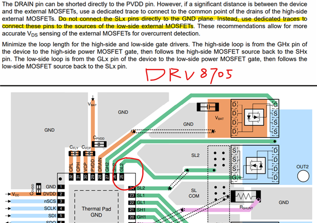
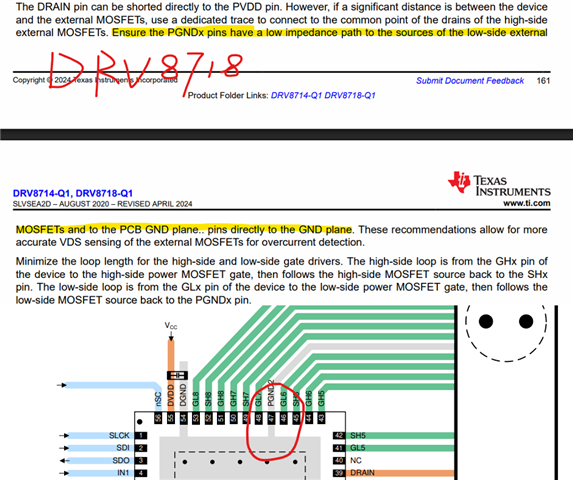
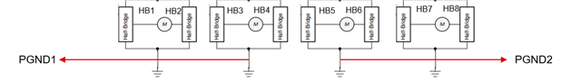
Compared to the DRV8705, both half-bridge drivers have corresponding SL (SL1 & SL2). The DRV8718 has 8 half-bridge drivers, but only 2 pins similar to the SL of the DRV8705 (PGND1 & PGND2), which creates a layout issue. If we also pull a single wire from the S terminal near the lower bridge MOSFET to the SL like with the DRV8705, the DRV8718 will have 8 half-bridge MOSFETs connected, and sometimes they may be relatively dispersed, making it impossible to ensure that each half-bridge's lower MOSFET's G and S terminals have small loops. I looked at the DRV8718 datasheet, which recommends that the PGNDx pins be grounded directly; based on our actual design, I propose the following design. Please help me check if it is reasonable.
1. Ground the PGNDx pins through a nearby hole close to the IC;
2. Since we are using a multi-layer board design, there is a complete GND layer, and the grounding holes for PGNDx will only connect to the GND layer while being disconnected from GND networks on other layers (the GNDs on other layers may be fragmented to some extent, making them not sufficiently continuous or complete, and I am concerned that this may interfere with PGND).
Thanks
Regards,
Daniel