This thread has been locked.

If you have a related question, please click the "Ask a related question" button in the top right corner. The newly created question will be automatically linked to this question.

DRV8363-Q1EVM: Pinout question – HALL_C signal

Part Number: DRV8363-Q1EVM
Other Parts Discussed in Thread: LP-MSPM0G3519, , DRV8363, DRV8363-Q1, LAUNCHXL-F280049C

Tool/software:

Hello,

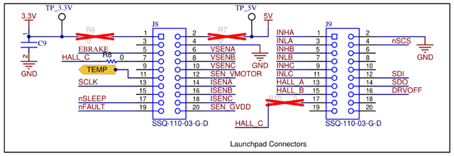
I am looking at the compatibility of the DRV8363-Q1EVM with the LP-MSPM0G3519 EVM. I have an issue with the HALL_C signal. How should one read the below schematic? Is this signal available both from the J8.7 and J9.17 pins? Why is it crossed out for J9.17? Actually, it would be good to have HALL_C available for J9.17 for the compatibility with the LP-MSPM0G3519 EVM because it is an analog pin when J8.7 is not.


Best regards,
François.

  • Hi,

    I have pursued my analysis using slvud90 page 14 and slau947 page 10 as reference schematics, and came up with the below. Please confirm if my analysis is correct, especially with the connector pins that I think are incompatible between both boards.

    DRV8363 pin

    DRV8363 pin type

    Compatible?

    LP-M0G3519 pin type

    LP-M0G3519 pin

    1 – 3.3V

    3.3V power

    Yes–Disconnect R6

    3.3V power

    1 – 3.3V

    3 – NC


    n/a


    2 – PA14

    5 – EBRAKE

    Digital

    Yes

    GPIO

    3 – PA9

    7 – HALL_C

    Analog

    No

    Digital

    4 – PA8

    9 – NC


    n/a


    5 – PB29

    11 – TEMP

    Digital

    Yes

    GPIO

    6 – PA25

    13 – SCLK

    SPI clock

    Yes

    SPI1_SCK

    7 – PB31

    15 – NC


    n/a


    8 – PB30

    17 – nSLEEP

    Digital

    Yes

    GPIO

    9 – PC2

    19 – nFAULT

    Digital

    Yes

    GPIO

    10 – PC3

    DRV8363 pin

    DRV8363 pin type

    Compatible?

    LP-M0G3519 pin type

    LP-M0G3519 pin

    2 – 5V

    5V power

    Yes–Disconnect R7

    5V power

    21 – 5V

    4 – GND

    Ground

    Yes

    Ground

    22 – GND

    6 – VSENA

    Analog

    Yes

    Analog

    23 – PA27

    8 – VSENB

    Analog

    Yes

    Analog

    24 – PA26

    10 – VSENC

    Analog

    Yes

    Analog

    25 – PB24

    12 – SEN_VMOTOR

    Analog

    Yes

    Analog

    26 – PB25

    14 – ISENA

    Analog

    Yes

    Analog

    27 – PB26

    16 – ISENB

    Analog

    Yes

    Analog

    28 – PB27

    18 – ISENC

    Analog

    No

    GPIO

    29 – PB10

    20 – SEN_GVDD

    Analog

    Yes

    Analog

    30 – PA15

          DRV8363 pin

    DRV8363 pin type

    Compatible?

    LP-M0G3519 pin type

    LP-M0G3519 pin

    1 – INHA

    PWM

    Yes

    TIMA0_C0

    40 – PB3

    3 – INLA

    PWM

    Yes

    TIMA0_C0N

    39 – PB9

    5 – INHB

    PWM

    Yes

    TIMA0_C1

    38 – PC4

    7 – INLB

    PWM

    Yes

    TIMA0_C1N

    37 – PC5

    9 – INHC

    PWM

    Yes (C0/C1 same conf)

    TIMA1_C0

    36 – PB4

    11 – INLC

    PWM

    Yes (C0/C1 same conf)

    TIMA1_C1N

    35 – PB5

    13 – HALL_A

    Analog

    No

    Digital

    34 – PA10

    15 – HALL_B

    Analog

    No

    Digital

    33 – PA11

    17 – NC


    n/a


    32 – PA12

    19 – NC


    n/a


    31 – PA13

          DRV8363 pin

    DRV8363 pin type

    Compatible?

    LP-M0G3519 pin type

    LP-M0G3519 pin

    2 – GND

    Ground

    Yes

    Ground

    20 – GND

    4 – nSCS

    GPIO

    Yes

    GPIO

    19 – PA7

    6 – NC


    n/a


    18 – PB6

    8 – NC


    n/a


    17 – PA30

    10 – NC


    n/a


    16 – RST

    12 – SDI

    SPI

    Yes

    SPI1_PICO

    15 – PB8

    14 – SDO

    SPI

    Yes

    SPI1_POCI

    14 – PB7

    16 – DRVOFF

    GPIO

    Yes

    GPIO

    13 – PB12

    18 – NC


    n/a


    12 – PB11

    20 – NC


    n/a


    11 – PB14

    Thank you.


    Best regards,
    François.

  • Hey Francois,

    The DRV8363-Q1 EVM was built for compatibility with LAUNCHXL-F280049C. In one of our initial revisions we had challenge running HALL C to J9.17.

    The Hall signal would not toggle which affected Hall based commutation. Therefore, We moved it to a different location (which we knew worked based on previous EVMs).

    I am looping in MSP team to comment on any potential challenges with this arrangement.

    Best,

    Akshay

  • Hi François, 

    If there remained the resistor on EVM (R6/R10), then it can be worked with LP-MSPM0G3519, as user can manually remove R6 and add R10 in the EVM board.

    Hall signal is digital signal, so it can be used with PA10/PA11/PA12.

    PB10 doesn't works for ADC function, there requires additional wire connected externally to the pin supports ADC function and not used.

    B.R.

    Sal

  • Hi Akshay and Sal,

    Thank you. I was mistaken in the nature of the Hall signal. So, only ISENC/PB10 should be wired separately, plus R6/R10 taken care of.


    Best regards,
    François.