This thread has been locked.

If you have a related question, please click the "Ask a related question" button in the top right corner. The newly created question will be automatically linked to this question.

DRV8874: Question for the actual copper area for RθJA selection in detailed design procedure of data sheet

Part Number: DRV8874
Other Parts Discussed in Thread: STRIKE, DRV8873, DRV8244-Q1, DRV8243-Q1, DRV8245-Q1

Tool/software:

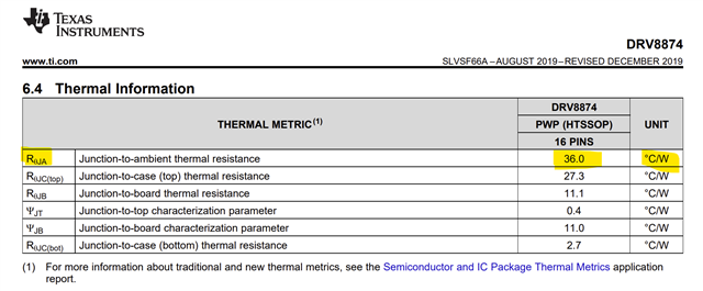
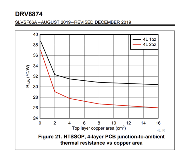
I read the detailed design procedure in datasheet as reference for my design.  The example uses 35C/W as RθJA, but does not indicate the copper area applied for this example directly. 

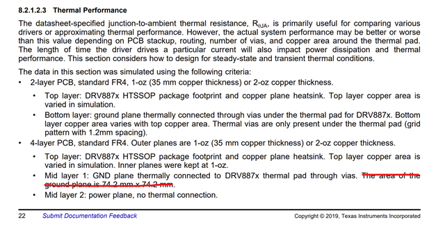
I get the copper area information in page 22:

"

  • 4-layer PCB ...

...

Mid layer 1: GND plane thermally connected to DRV887x thermal pad through vias. The area of the
ground plane is 74.2 mm x 74.2 mm.

...

"

It looks like "74.2mm x 74.2mm" to be the copper area for  RθJA of 35C/W.  

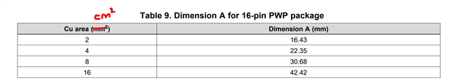
However when I continue the reading , in page 23, Table 9 indicate that for 4 layer, the board dimension is 22.35x22.35.  So I am confused with the actual copper area in this example. 

May some one can explain to me the actual copper area in this example?

  • Hi Myles,

    Thanks for your question.

    See below thermal specifications in the datasheet. RθJA specification follows JEDEC standards for test methods. Also review the application note highlighted underneath these specifications. The JEDEC test card for this package uses 2s2p 4L 2 oz Cu top and bottom and 1 oz Cu inner layers PCB. Exact dimensions of JEDEC standards cannot be published here. It can be purchased from JEDEC if needed. This RθJA value is used in the example you mentioned. However I see a small typo, uses a value of 35 instead of 36. Most of the example calculations in several of our datasheets may use this RθJA specification provided in the Thermal Information for the device which always follows JEDED standards. All IC vendors follow JEDEC to help users compare thermal performances with a common standard.     

    That said, you won't need the JEDEC test card details to design a desired PCB for this device. Follow the recommendations from section 8.2.1.2.3 Thermal Performance. Simulation conditions are mentioned in this section. As well as you can see section 8.2.1.2.3.1 Steady-State Thermal Performance and section 8.2.1.2.3.2 Transient Thermal Performance plots for various board types and Cu area. These are done with thermal modeling and simulations. You can see steady state thermal performance RθJA varies with Cu area. 


    The EVM PCB design Altium project and schematics are available for download from the EVM webpage which will simplify your PCB design. Thank you.

    Regards, Murugavel 

  • Hi,

    Thanks for your detailed response. I had considered to refer to the performance plot (RθJA Vs. Cu area) in datasheet,  but the 36C/W value is for lower copper area, that does not reflect the actual copper area in the example.  My design will provide 70*40mm cu area/1 oz for heat dissipation, it is out of the plot range, but it looks like the RθJA value is close to 30C/W, however your example has much larger cu area (74mmx74mm), but still use 36C/W as RθJA. Therefore I am a little curious what RθJA value I should select.

    Additionally, DRV8874 is rated for 6Amp output current, but HS/LS Mosfet Rds(on) is 120mOhm at maximum. It does mean there will be high power consumption(8.6Watt) in either clockwise or anti-clockwise direction that definitely lead to high temperature in junction no matter how much copper area/thickness we use (performance curve becomes flat after a certain Cu area value.).  may I know how we can use  DRV8874  in an application that require 5~6A continuous output?

  • Hi Myles,

    however your example has much larger cu area (74mmx74mm), but still use 36C/W as RθJA. Therefore I am a little curious what RθJA value I should select.

    The example calculation in section 8.2.1.2.2 Power Dissipation and Output Current Capability does not explicitly mention Cu area. The calculation considers the RθJA from the datasheet specification (JEDEC) so JEDEC test card dimensions could be assumed. 

    The 8.2.1.2.3 Thermal Performance section is not connected to the example calculation in the previous section of the datasheet. The below sentence (red strike in the below snapshot) looks to be incorrect. Likely typo carried over from HTSSOP 24-pin package. The DRV8874 has a smaller HTSSOP 16-pin package. Please ignore that sentence. The board dimensions used in simulations are provided in Table 9. Dimension A for 16-pin PWP package in the datasheet. For the highest Cu area 16 mm2 in the table, the PCB dimensions considered are 42.42 mm x 42.42 mm, according to the table. 

    I also noticed the table has a significant typo. See below. I have noted these corrections for our next update cycle. 

    Your PCB 70 mm x 40 mm Cu area would be < 28 cm2. With some extrapolation of the plot, RθJA looks to be about 30 °C/W. You can substitute this value for the thermal estimation calculation. Note, these calculations are provided for estimation purpose only. The actual die temperature could be higher.   

    Regards, Murugavel 

  • Hi Murugavel ,

    Thanks for your clarification.  I assume there are some typo err in this datasheet, but not sure. :-)

    My last open question is that if you think  DRV8874 is really suitable for the 5-6A application, that is one of the reasons I consider to select this chip. or May you give me an acceptable maximum current in the dimension of my PCB, 3A or 4A? I do not have forced air flow across the surface of the board.

  • Hi Myles,

    The specification in the DRV8874 datasheet 6 A peak can be supported only for very short durations. If you are looking for continuous 6 A application this would not be the device for you. Even with the DRV8873 it would depend on supply voltage, ambient temperature etc. You could drop in the thermal formulae in to an Excel and do what if analysis. 

    You can also take a look into the DRV8243-Q1, DRV8244-Q1 and the DRV8245-Q1 datasheets, their product page also carries an Excel calculator for die temperature estimation - see below. You can use this tool to see which device would support the desired load current and duration with or without PWM control using this Excel. 

    Regards, Murugavel 

  • Hi Murugavel,

    I check the calculation excel you recommend, regarding the Rds(on) value, is it for LS and HS or for the sum of LS and HS?

  • Hi Myles,

    It is for the sum of LS + HS, mentioned in the header of that column. Thanks.

    Regards, Murugavel