This thread has been locked.

If you have a related question, please click the "Ask a related question" button in the top right corner. The newly created question will be automatically linked to this question.

DRV8305-Q1: About Wake pin.

Part Number: DRV8305-Q1
Other Parts Discussed in Thread: DRV8305

Tool/software:

Hi Expert,

Have a nice day! I have question need your professional support:

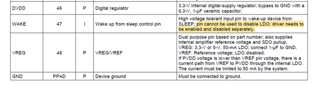
For DRV8305-Q1, I don’t fully understand about the description of WAKE Pin.

What does “pin cannot be used to disable LDO; driver needs to be enabled and disabled separately.” mean?

Thanks!

Best Regards,

Leo

  • Hi Leo,

    Here is a clearer description of the WAKE pin functionality:

    The sleep state can be entered by issuing a sleep command through the SLEEP bit in SPI register 0x9, bit D2 with the device in its standby state (EN_GATE = LOW). The device will not respond to a sleep command in its operating state.

    The device can then only be enabled through the WAKE pin which is a high-voltage tolerant input pin. For the DRV8305 to be brough out of sleep, the WAKE pin must be at a voltage greater than 3 V. This allows the wake pin to be driven, for example, directly by the battery through a switch, through the inhibit pin (INH) on a standard LIN interface, or through standard digital logic. The WAKE pin will only react to a wake up command if PVDD > VPVDD_UVLO2. After the DRV8305 is out of SLEEP mode, all activity on the WAKE pin is ignored.

    In regards to the sentence "pin cannot be used to disable LDO; Driver needs to be enabled and disabled separately", This means that EN_GATE is the driver enable and disable, and WAKE pin cannot be used like a regular sleep pin which can be found on our other devices. The WAKE pin will only remove the device from the sleep mode condition.

    Thank you,

    Joseph

  • Get it.

    Thanks for your detailed response.

    Best Regards,

    Leo