This thread has been locked.

If you have a related question, please click the "Ask a related question" button in the top right corner. The newly created question will be automatically linked to this question.

DRV8889-Q1: The chip manual has a sleep pin. How should it be set during communication

Part Number: DRV8889-Q1

Tool/software:

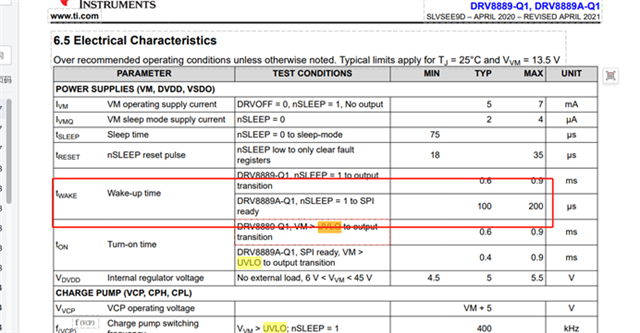
The first frame of SPI communication was faultless. Later on, the chip manual has a maximum time of 200 seconds from the sleep pin to SPI communication. Do we need to pull the sleep pin up and down each time we communicate?

  • Hi Bao,

    Thank you for the question.

    See below from the datasheet. For SPI communication the nSLEEP must be HIGH, device awake. After the rising edge of the nSLEEP prior to the first communication after wake up the MCU must wait tWAKE before doing an SPI transaction. For the DRV8889A-Q1 device tWAKE is 200 μs max. For the DRV8889-Q1 tWAKE is 0.9 ms max. 

    Do we need to pull the sleep pin up and down each time we communicate?

    No. If the device goes to sleep nSLEEP = 0 all the written config registers will be reset to their default state. Once awake after writing the config registers the device must stay awake. If the device goes to sleep and wake up the config registers must be reconfigured again.

    The nSCS pin must be taken HIGH between every SPI transaction frame. See below from the datasheet. Thank you.

    Regards, Murugavel