This thread has been locked.

If you have a related question, please click the "Ask a related question" button in the top right corner. The newly created question will be automatically linked to this question.

DRV8350: DRV8350 damage in GHA/SHA (U phase)

Part Number: DRV8350

Tool/software:

Dears,

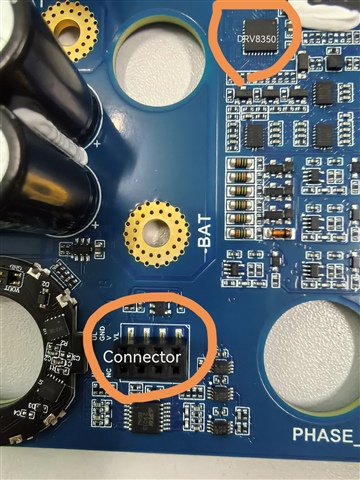
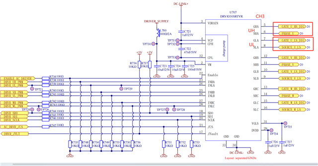
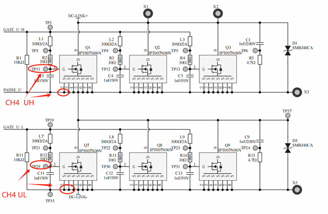
  The customer uses DRV8350 in the application scenario of electric forklifts, with a 24V system and a three-phase asynchronous motor as the load. The motor power ranges from 1.5KW to 3.0KW. Use DRV8350SRTVR to drive MOSFETs (each half bridge arm is used in parallel with 3 Infineon IPT007N06N). The Qgd of a single Infineon IPT007N06N is 39nC, and the Qgd of three in parallel is 117nC. According to DRV8350 manual 9.2.1.2.2, the Idrivep range is calculated to be 390-1170mA, and the Idriven range is 780-2340mA. The Idrivep set on the software is 600mA, and the Idriven is 1300mA, which meets the requirements.


  During the vehicle reinforcement test, the 3.0KW model was tested for more than 30 hours without any abnormalities; However, the 1.5KW model underwent three consecutive reinforcement tests and all showed DRV8350 damage. The malfunction occurred during several hours to over ten hours of vehicle testing, all of which occurred during the process of carrying the vehicle forward.


   Check the software, read the register, and display GDF. The driving current of the bridge arm on phase U is too high; Check the hardware, three times there was a short circuit or low impedance between pins GHA and SHA of DRV8350, while all other components were normal. Check LAYOUT and no abnormalities have been found in the three half bridge drive signal lines. May I ask under what circumstances this GDF may occur? What are the directions for troubleshooting problems?

   Thanks.

  • Hey Jon,

    1) Who is the customer?

    2) Is this the first design/prototype?

    3) Just to confirm the damage always occurs on Phase A? Is this the phase farthest from the driver on your layout?

    4) Can you send schematic?

    5)At what point in nFault triggering? Any waveforms with nfault and GHA, SHA signals, VGS?, What is your VDS slew time both rise and fall?

    6) During high current operation can you take waveforms of GHA, SHA, VGS, Vdrain? And a waveform showing INHA, GHA, VGS, nfault and trigger on nfault during GDF fault?

    7) What is the Tdrive setting?

    Also if you attached images, in the original post I am unable to open them. so please try attaching again or sending a zip folder with labeled images (showing signal name, voltage levels, and time scale)

    Best,

    Akshay

  • Akshay,

        Pls see my comment,thanks.

    1) Who is the customer?

    -----Linde FENWICK

    2) Is this the first design/prototype?

    -----First design

    3) Just to confirm the damage always occurs on Phase A? Is this the phase farthest from the driver on your layout?

    ----Yes, pls see the PCB in attechment.

    4) Can you send schematic?

    -----Pls see the Sch in attechment.

    5)At what point in nFault triggering? Any waveforms with nfault and GHA, SHA signals, VGS?, What is your VDS slew time both rise and fall?

    ------Randomly appearing, the operating condition is when the motor is fully loaded(1.5KW) and driving forward, GHA, SHA signals, There is currently no waveform available (waveform needs to be captured). The waveform has been tested on the bench, as shown in Excel Table 3

    6) During high current operation can you take waveforms of GHA, SHA, VGS, Vdrain? And a waveform showing INHA, GHA, VGS, nfault and trigger on nfault during GDF fault?

    -----Because the malfunction occurs during vehicle operation, it is difficult to capture waveforms in the driving environment. The waveform on the test bench is attached for your reference. Do you have any suggestions?

    7) What is the Tdrive setting?

    ----4000ns

    KWPC07_DRV8350_SCH PCB wave form.xlsx

  • Hey Jon,

    Thanks, I will go through this and provide feedback.

    Best,

    Akshay

  • Akshay,

         Customer is very urgent,could you pls help?Thanks.

  • Akshay,

        Update some informance:

    1.DRV8350 Register setting:

    driver_control 0x401

    driver_gate_hs 0x39a

    driver_gate_ls 0x39a

    driver_ocp:0x16a

    2.Only Gate Drive HS is overcurrent and LS is ok.

    3.if customer reduce the setting of IDRIVEP_HS and IDRIVEN_HS, can reduce the probability of malfunctions.Now IDRIVEP_HS and IDRIVEN_HS is 600mA and 1300mA.But if reduce IDRIVEP_HS and IDRIVEN_HS,will increase switch losses. Now the switch loss has exceeded the customer's target, and the customer hopes to reduce the switch loss, so they cannot increase the Idriver, and even hope to increase it.

    4.mosfet is in the other power board,and connected with the connector in the main board.


  • add a point: only DRV8350 damaged and mosfet is good.

  • Hey Jon,

    Sorry, I was out of office.

    Could you tell me what the following signals are:

    CH2: TC377 output driver
    CH3: DRV8350 output driver      
    CH4: MOSFET gate PIN signal

    For the waveforms I requested please take them as close to the driver pin with respect to driver ground. As if the signals is taken near the MOSFET,  capacitance of the MOS can affect the signal and smooth it out. We are concerned with driver abs max violations.

    Best,

    Akshay

  • Hey Jon,

    This document seems the same as earlier one, what was the update?

    My questions/clarification need was

    1) what is the TC377 output driver on the schematic

    2) DRV8350 output driver (is that GHx-shx or , SHx-gnd?)

    3) what is mosfet gate pin signal (GHz-shx at mosfet? glx-gnd at mosfet?) 

    This is why I was requesting the specific signals combinations I mentioned in my earlier post being measured at the driver pin to see if we see any abs max violation. Also I dont think Shx-gnd is shown as I dont see a signal at 24V in the existing waveforms

    Please let me know if i missed anything.

    Best,

    Akshay

  • Akshay,

      Please refer to the indicates in the picture.Thanks.

  • Hey Jon,

    Thanks for the clarification for ch1, and ch2. 

    Where is Channel 3?

    Also there is a lot of noise in the gate signal which might coincide with an SHx slew of another phase. Therefore, slowing down the VDS slew using lower Idrive/gate resistor will be recommended.

    if you can provide the wave captures I requested  (with approx 100ns/div )then we can see the SHx and GHx behavior.

    Best,

    Akshay

  • Akshay,

         pls see the picture of Channel 3.

         Because lower Idrive/gate resistor will increase switch losses,and the switch losses now is higher than the target,so can't reduce the Idrive/gate.

         TI Local FAE stone suggest removing the 1nF capacitor and magnetic beads from the Mosfet gate. The customer found that after removing this 1nF capacitor, it ran for 30 hours without any further problems. The customer inquired whether removing this capacitor would have any other adverse effects? Is this plan feasible? Thanks

  • Hey Jon,

    Where is the ferrite bead placed?

    let me check with the team as well.

    Best,
    Akshay

  • Hey Jon,

    I would need the waveforms I requested to better understand the situation. Also how many units were tested after removing the ferrite bead and the VGS cap?

    Do we have gate, source waveforms before and after removing the cap and bead?

    Where is the ferrite bead placed? Also if we change two items it is hard to tell which specific change led to the improvement.

    Please help clarify, thanks!

    best,

    Akshay