Tool/software:
Hello! Dear. TI Team,
We are currently using the DRV8350RH gate driver IC and are experiencing two issues.
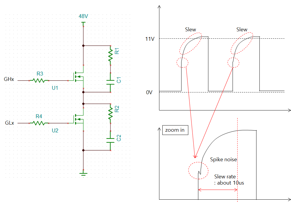
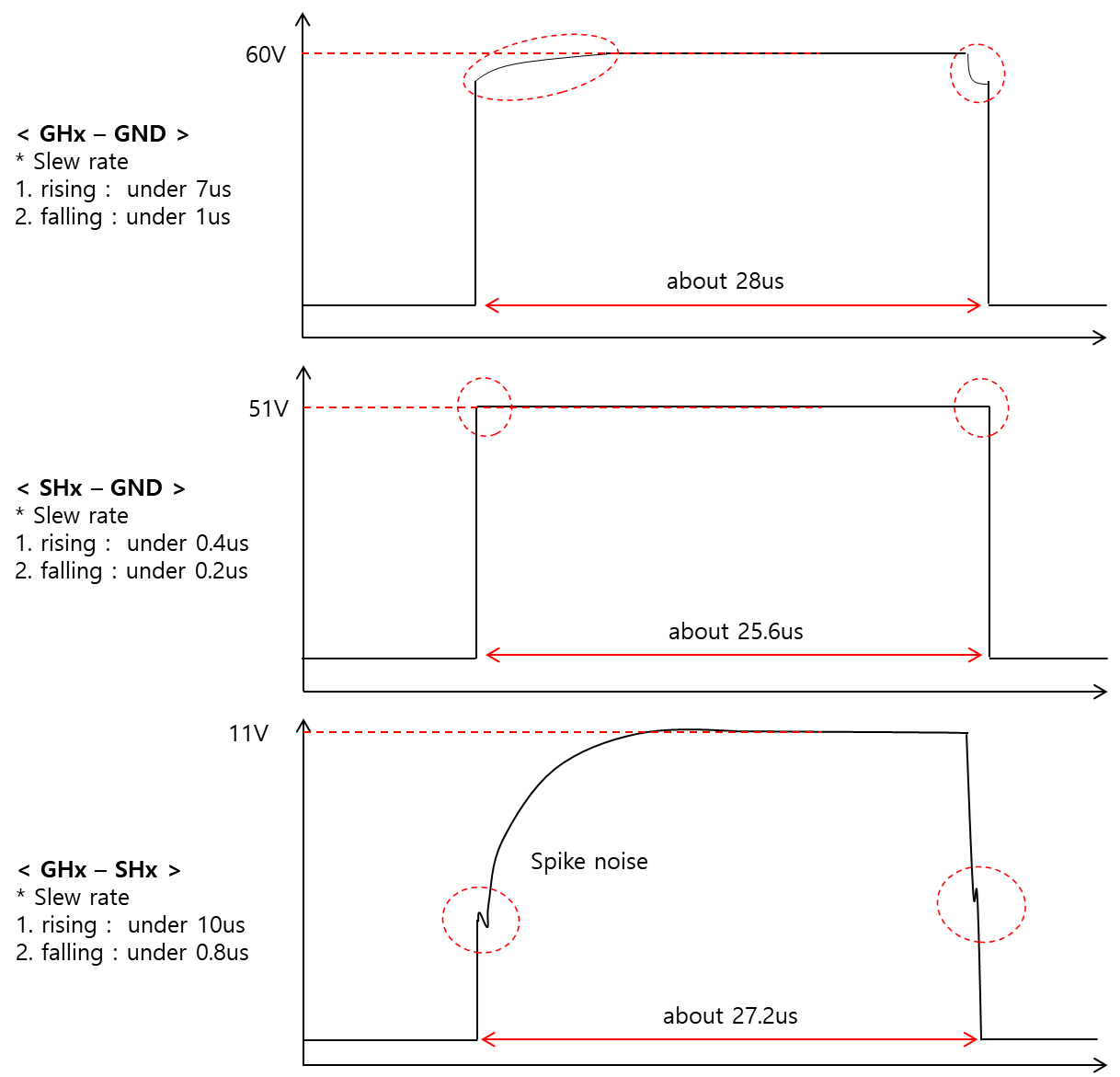
We have configured the MOSFETs for driving a 3-phase motor as shown below, and we are applying a snubber circuit.
First, we measured the VGS of the high-side MOSFET using a differential probe, and the measured waveform is attached.
-
The VGS (GHx) waveform of the high-side MOSFET appears to be a square wave, but the positive edge section shows a slight slew rate. However, the VGS (GLx) of the low-side MOSFET is a perfect square wave with no slew rate.
We would like to know if it is normal for only the high-side MOSFET’s VGS (GHx) waveform to have a slight slew rate in the positive edge section, and why this slew region occurs. -
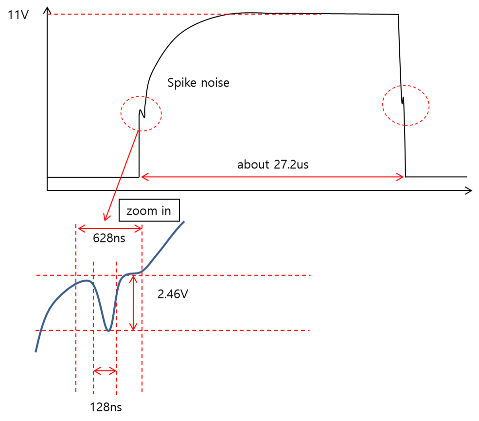
When zooming in on the positive edge section of the high-side MOSFET’s VGS (GHx) waveform (which has the slew rate), we observe a small spark-like noise.
We would like to know possible methods to eliminate this phenomenon, the reasons why it occurs, and what side effects it may cause if it persists. (IDRIVE PIN : SHORT TO GND (Minimum setting)) - R3, R4 = 1ohm / R1, R2 = 3ohm / C1, C2 = 470pF
Thank you, as always, for your kind support.
Best regards,