DRV8876-Q1: Testing failure modes

Part Number: DRV8876-Q1
Other Parts Discussed in Thread: DRV8876, DRV8876EVM

Tool/software:

Hello Team,

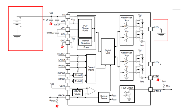
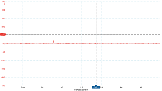
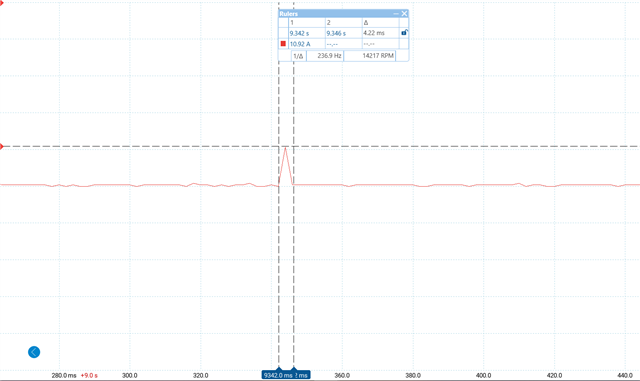
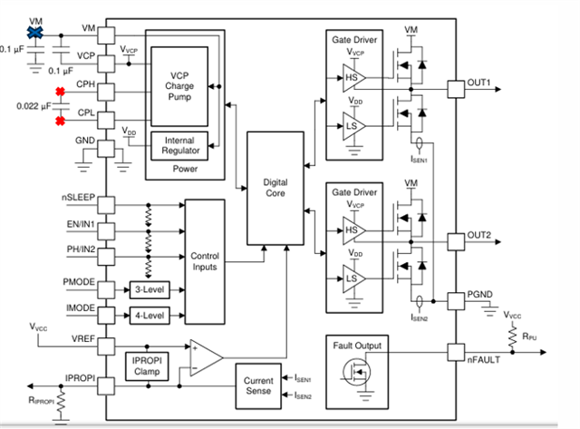
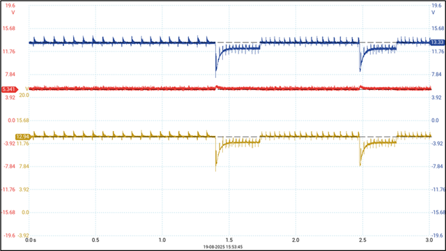
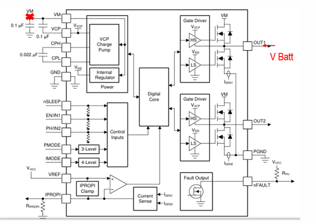
I have been testing the DRV8876 for my application, as a part of it we connected VDC(+12V) to VM and negative terminal to OUTA and the GND and PGND terminal were floating. Initially the a high current of 13A pulse is drawn by the circuit later no changes were observed. The IC tested and it found in good condition, I couldn't understand how it changed it's behavior of the circuit? Can the fault pin can trigger without any reference point(GND/PGND)?

Regards,

Jishnu K

  • Hi Jishu,

    Could you provide a rough block diagram of the setup, just want to make sure I'm not misunderstanding the setup? Also please include any inputs to the device during this test condition

    Regards,

    Joshua

  • Hi Joshua,

    The below given is the test:

    The idea is to experiment the fault situation where the GND terminal is connected to output terminal instead of ground pin. The reference ground will be floating and the output terminal will be connected to the ground. The current wave form drawn from the battery is given below. The current peak is 13A and the pulse duration is 3ms.

    Hope this will help you.

    Regards,

    Jishnu K

  • Hi Jishnu,

    Thank you for the additional explication, please allow me a couple of days to look into what path the current is taking.

    Regards,

    Joshua

  • Hi Joshua,

    Any update on this issue.

    Looking forward for your response.

    Regards,

    Jishnu 

  • Hi Jishnu,

    Apologies, I have not had time to get around to looking into this. I will aim to provide a response tomorrow.

    Regards,

    Joshua

  • Hi Jishnu,

    I tested this on bench, and I believe the large current draw was likely from the bulk capacitance on VM. Was this test done on a DRV8876EVM?

    I would also like to ask if this scenario is causing any issues with the device or is this question just more out of curiosity? I will need to reach out to my internal team to determine the path the current is taking, floating GNDs makes this analysis a bit more difficult.

    Regards,

    Joshua

  • Hello Joshua,

    Thank you for the response.

    I did this experiment on a PCB made with my specification. Unfortunately, on some IC it is leading to the failure condition.

     Apart from this there is another test where the GND is connected and applying the VDC at the OUT1 (Similiar, but the VM is floating). This creating a backward current path, which I didn't expect due to because of the internal MOSFET diode. This is create a voltage at my power line which is connected to the other circuit and the operation of those circuits draws the current through the IC. This is leading to instant failure of the circuit. 

    I really appreciate if you can look into this situation, If it possible recommend some protection scheme from this kind of faults.

    Regards, 

    Jishnu K

  • Hi Jishnu,

    I will make sure to work with my team to determine a protection scheme. I will aim to provide you in a week.

    Regards,

    Joshua 

  • Hello Joshua,

    Greeting of the day. Any update on query. 

    I would also like to know whether the current regulation and control mode has some impact on it or not. Currently I'm using static switching with fixed off time and automatic retry.

    Regards,

    Jishnu K

  • Hi, 

    Thank you for your post. Monday September 1st is national holiday in US. Please expect delay or please wait for our expert assignment on Tuesday US time.

  • Hi Jishnu,

    I am still working with the design team on this issue I will provide you a status update at the end of the week.

    Regards,

    Joshua

  • Hi Jishnu,

    1. Can a zoomed in capture of the 13A peak pulse be provided?
    2. Can a capture of the VM voltage and device GND voltage (so PGND and/or GND pins) be provided? We are looking to see how much the GND of the device is jumping during this event

    Regards,

    Joshua

  • Hello Joshua,

    Please find the response for your queries:

    1.Can a zoomed in capture of the 13A peak pulse be provided?

    The above figure shows a current pulse during that event. It is observed that the value is 10A for a duration of 4ms when it failed.

    2. Can a capture of the VM voltage and device GND voltage (so PGND and/or GND pins) be provided? We are looking to see how much the GND of the device is jumping during this event.

    I'm attaching the waveforms during the experiment when the Vdc is connected to the OUTPUT of DRV8876  and ground is connected . The voltages at different terminals are taken as shown below.

    The voltages are probed at VM(blue waveform), across charge pump(red waveform) and the main power line(yellow) which are connected to the other circuit

    Hope this will help.

    Regards,

    Jishnu K

  • Hi Jishnu,

    1. What does other circuit mean, just want to make sure I am not misunderstanding what you mean with this statement?
    2. Were you able to capture the voltage between the negative terminal of the 12V supply and one of GND pins of the DRV8876? 
    3. When the device gets damaged, what pin becomes shorted or becomes open?

    I will share this information with the team. I will aim to provide an update middle of next week.

    Regards,

    Joshua

  • Hello Josua,

    Kindly find the response below:

    1.What does other circuit mean, just want to make sure I am not misunderstanding what you mean with this statement?

           Ans:


     There is another test case where the VM is kept floating and the output is connected to the battery voltage. This test case lead to instant failure of the circuit. The previous waveforms are result seen in that circuit.

    2. Were you able to capture the voltage between the negative terminal of the 12V supply and one of GND pins of the DRV8876? 

    Ans: No, I will collect and share as soon as possible.

    3.When the device gets damaged, what pin becomes shorted or becomes open?

    Ans. The damages seen in Vm and VCP terminals . A  pins are seen in short and burnt condition.

    Regards,

    Jishnu K

  • Hi Jishnu,

    Thank you for quickly providing the additional information.

    I want to confirm, how much capacitance is on the VM pin on the board this testing has been done on? 

    Regards,

    Joshua

  • Hi Joshua,

    The Vm terminal is connected to a 12V bus. A 0.1uF/50 is connected near to the DRV8876, apart from that a 330uF is connected as a bulk capacitance in  12V power line.

    Regards,

    Jishnu