DRV8305-Q1: Input current too high after setting EN_GATE

Part Number: DRV8305-Q1
Other Parts Discussed in Thread: DRV8305

Tool/software:

Hello,

I have had this issue once before:

https://e2e.ti.com/support/motor-drivers-group/motor-drivers/f/motor-drivers-forum/1135604/drv8305-q1-high-current-after-setting-gate_en

and the problem was easily solved, since the VCPH to PVDD cap at 2.2nF and not the recommended value of is recommended to be 2.2uF.
After changing the cap to the right value, everything was okay.

Now, I have a similiar issue on a new revision of the same board. The only things that have change
are a reduction in the size of the cap for CP1 and CP2 from 0603 to 0402, and an update to the
new land pattern as described in the Datasheet SLVSD12D. The current to the board is at 77 mA
when the EN_GATE is cleared and when set jumps to 318 mA where we would expect 150 mA as
in the earlier version of the board.

I have checked the sizing of the passives around the part, set the IDRIVE currents to minimum,
looked for any mistakes in the new footprint and I do not see the mistake.
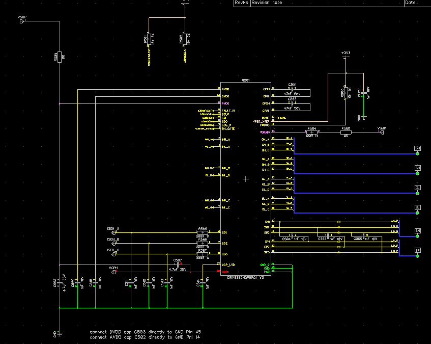
Here the Schematic:

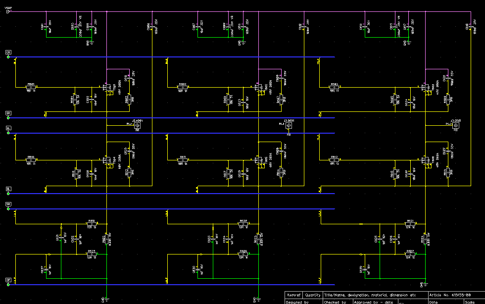
and the schematic of the power stage:

Neither the chip nor other parts are exceptionally hot, but maybe 2 °C warmer as compared to the earlier version of the board.

Any Ideas are much apprecitated.

Kind Regards,

John

  • Hi John,

    Although the schematic is a little unclear, it looks like VCPH to PVDD cap is 4.7uF with a 35V rating?

    In the previous E2E it was mentioned that the rating should be PVDD x 2. It could be that your capacitor is being de-rated?

    can 0603 caps fit on your board for CP1 and CP2? This would be a good test to do is seeing the behavior on the same board with the different sized capacitors.

    Regards,

    Yara

  • Hello Yara,

    Thank you for your fast response. Sorry for the low resolution of the schematic. If you need, please let me know how I can send you the schematic in a higher resolution.

    The VCPH to PVDD cap used is a takeover part from the board where the DRV8305-q1 is working as expected. From the previous E2E, I understand that CP1 should be rated for PVDD and CP2 should be rated for PVDD x2. Both of the caps CP1 and CP2 are rated for 50 V.

    In the previous E2E, I have not seen a rating for the cap VCPH to PVDD x 2. The datasheet for the DRV8305 SLVSD12D is showing 2,2 μF rated for 16 V for the VCPH to PVDD cap:

    Please confirm PVDD x2 for VCPH to PVDD cap.

    Good idea to try the 0603 size for CP1 and CP2. I soldered in the 0603 caps yesterday, but unfortunately no improvement. :-(

    I have checked the values of these parts and measured in circuit with an LCR meter to confirm. Everything seems to fit.

    On this version of the board, I have also closely followed the layout guidelines in section 10.1 of the datasheet.
    So in this version:

    • the DVDD and AVDD 1 μF caps are connected directly to the adjacent GND pins of the DRV8305-Q1
    • CP! and CP2 are placed dorectöy mest tp tje DRV8305-Q1 charge pump pins
    • The VCPH 2.2-μF and VCP_LSD 1-μF bypass capacitors are placed close to their corresponding pins
      with a direct path back to the DRV8305-Q1 PVDD for VCPH and GND for VCP_LSD
    • The PVDD 4.7-μF bypass capacitor is placed as close as possible to the DRV8305-Q1 PVDD supply
      pin
    • footprint was updated to the version in the datasheet Revision D
    • The loop length for the high-side and low-side gate drivers have been minimized
    • The VDRAIN pin is routed through a 100-Ω series resistor directly to the MOSFET DRAIN

    Here is a picture of the layout:

    I have checked everything again and again and have not found the mistake. Could it be in the new foot print?

    Kind Regards,

    John