DRV110: The DRV110 model dosen't work

Part Number: DRV110

Tool/software:

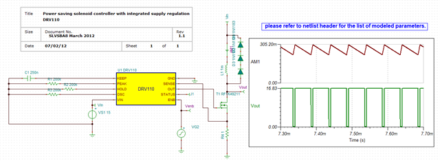
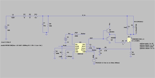
Hello, I'm trying to simulate the DRV110 in LTspice but seems that there is something wrong in the model, in pratical the regulation of the PWM is not like is aspected to be, here the test circuit:
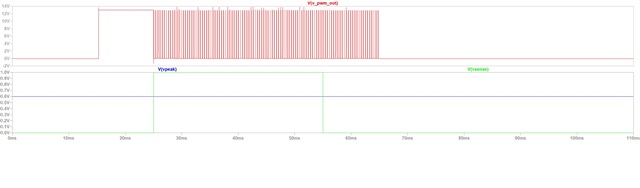
.

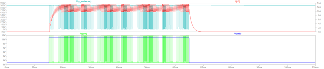
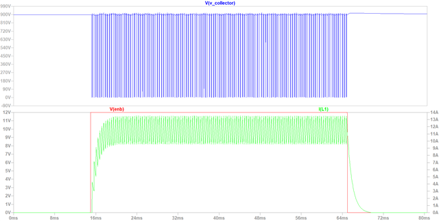
We can see that when the sense signal is lower than the Vpeak level the output goes high and when the sense signal is higher than the Vpeak  the DRV110 reduce the duty cycle to 10% max, but when the sense signal go down to the Vpeak level the dudty cycle doesn't change and stay at 10%. 
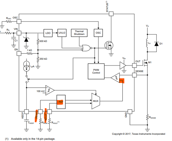
On model lib file:

* If Vsense is smaller than Vref, a high will be generated at
* OUT pin.
* When Vsense is greater than Vrefs, OUT pin  will generate a *  * 10% duty cycle signal

What is wrong? How to fix it?

Thanks

antonio

  • Hi Antonio, 

    Thank you for reaching out to us. 

    The circuit is not developed correctly. Would you please modify your cicurui using DRV110 TINA-TI Reference Design (Rev. A) shared by TI. To select appropriate value for components you need to use SLIC024  DRV1xx Device Parameter Selector   and choose the right value based on your application. 

    Best regards, 

    Mojtaba

  • Hi Mitaba,

    thanks for your fast answer, but the circuit is correct, we don't use the HOLD current in us application and it's work, but the simulation doesn't work.

    if I use the SLIC024 file I get the same components values we use

    Thanks

    antonio

  • Hi Antonio, 

    Thank you for your question.

    DRV110 has 8 pin and 14 Pin packages. Which one are you using in your application? The model you showed is for 14 pin packages.  

    You cannot leave HOLD pin unconnected in DRV110 14 pin packages. As shown below, The Vsense after tkeep is compared with Vref which is determined by RHOLD. In the 8-pin package, the HOLD pin is not bonded out. For this package, the HOLD mode is configured to default (internal) settings. for Rsense 1 ohm is 50 mA. Please use DRV110 TINA-TI Reference Design (Rev. A) as a reference to correctly setup the  simulation. 

    Best regards, 

    Mojtaba.

  • Hi Mojtaba,

    Yes I use 8 pins DRV110 and so means I have to use a resistor, 200k according to calculation, connected to GND if I use the Pspice model, but still there is something it doesn't work  fine, I'm aspeting to have 40A current regulation....maybe I can't us ethe DRV110 model for Pscipe simulation?

    Thanks, 

    Regards

    antonio

  • Hi Antonio, 

    Could you please share the entire simulation schematic screenshot with me? I have a few questions regarding the setup. Specifically, I was wondering if you could clarify the value of Vv collectort - is it 900V?

    Additionally, I noticed that the current is set by Pulse generator on sense pin. Could you please explain why you used Vpulse connected to sense. as can be seen the output is switching which resulted a current lower than Peak current. Also the current switch from peak to hold current after keep time.  From my understanding, the pulse generator creates a fixed current, which is then adjusted based on VREF and Vsense to produce the output PWM. Could you please help me understand the reasoning behind this approach?

    Best regards, 

    Mojtaba.

  • Hi Mojtaba,

    Well the Vv collector could be whatever value it doesn't affect, but anyway the circuit with the V3 Pulse on sense is to see the behavior of the DRV110 model, is not the real circuit. Attach you can see the all LTspice circuit, I tried to upload the asc file but I can't, is it possible to do? 

    Thanks, regards

    antonio

  • Hi Antonio

    Based on your circuit, after enabling the device, it should provide a high current of 40 A for 220 ms, followed by a switch to hold current (5a). However, the enable pin is only high for 50 ms, which is insufficient time for proper operation. To troubleshoot, please capture the following signals: Vsense, Vpeak, Vhold, and IL current. We need to verify if the switching is performed correctly. Additionally, check the switching frequency to ensure it matches the set value of 20 kHz. you can also connect OSC pin to GND to have 20 KHz

    Best regards, 

    Mojtaba