DRV8889-Q1: step loss after power on and wake up from sleep mode

Part Number: DRV8889-Q1

Tool/software:

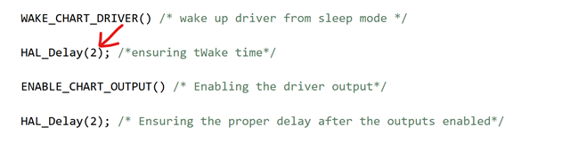
I am using an STM32 microcontroller with the DRV8889 driver to control a bipolar stepper motor. After power-up, the motor consistently misses the first two step pulses—it only starts moving from the third pulse onward (sometimes from second pulse). Additionally, when the driver is brought out of sleep mode, the motor does not respond to the first step pulse after wake-up

for (int i=0; i<1000; i++){

WAKE_CHART_DRIVER();

HAL_Delay(2);

ENABLE_CHART_OUTPUT();

_chart_steps_gpio(1, 1, 5);

step_count++;

DISABLE_CHART_OUTPUT();

SLEEP_CHART_DRIVER();

HAL_Delay(1000);

}

  • Hi Maheshwari,

    Thanks for your post.

    After power-up, the motor consistently misses the first two step pulses—it only starts moving from the third pulse onward (sometimes from second pulse). Additionally, when the driver is brought out of sleep mode, the motor does not respond to the first step pulse after wake-up

    See the below specifications from the datasheet. After power on or wake up from sleep you must wait > 0.9 ms, for example 1 ms before issuing STEP input pulses. Also SPI transactions won't be accepted until SPI ready. So it would be good practice to wait for 1 ms after power on or wake up from sleep, then do the necessary SPI configurations and then issue the STEP pulses for the motor rotation. Thank you.

    Regards, Murugavel 

  • Hi, thank you for the reply, actually I have given delay >1ms, as you can see in the code i have given 2ms delay

  • Hi Maheshwari,

    I have given delay >1ms, as you can see in the code i have given 2ms delay

    That's good. After this 2 ms delay and configuration of the device do you still miss the first two step pulses? Make sure the STEP input pin is logic LOW when the device is powered on or wake up from sleep. Before issuing STEP pulses the outputs must be enabled, DRVOFF pin LOW and DIS_OUT bit in CTRL2  is 0b. This is the default CTRL2.DIS_OUT for the DRV8889-Q1. For the DRV8889A-Q1 the default value is 1b, it must be changed. If you're using the non-A device the default value is good. 

    A drive STEP input must be a STEP input transition to HIGH and then transition to LOW, the index advances up or down depending on the DIR for every HIGH to LOW transition. See below information.

    Regards, Murugavel 

  • Hi Murugavel,

    I’ve tried the approach of ensuring the STEP pin is low before sending any step pulses. Additionally, I’m enabling the driver outputs prior to initiating the step pulses. Below is the code I’m using to initialize the driver. Could you please review it and let me know if you have any suggestions or alternative solutions?

    **I have used ramping technique for increasing the current, and also I have tried with directly the PWM instead of ramping by
       TIM1->CCR1 = 2000; (full duty cycle) 

    void power_on_chart_driver(void){

    TIM1->CCR1 = 0; /* vref = 0 */

    HAL_TIM_PWM_Start(&htim1, TIM_CHANNEL_1);

    HAL_Delay(10);

    for (int i=0; i<100; i++){ /* Ramping the current */

    TIM1->CCR1 = i*20;

    HAL_Delay(2);

    }

    HAL_Delay(10);

    HAL_GPIO_WritePin(step_GPIO_Port, step_Pin, GPIO_PIN_RESET); /* step pin Low state for init = 0 */

    HAL_GPIO_WritePin(dir_GPIO_Port, dir_Pin, GPIO_PIN_SET); /* dir pin Low state for init = 0 */

    WAKE_CHART_DRIVER() /* wake up driver from sleep mode */

    HAL_Delay(2); /*ensuring tWake time*/

    ENABLE_CHART_OUTPUT() /* Enabling the driver output*/

    HAL_Delay(2); /* Ensuring the proper delay after the outputs enabled*/

    }

  • Hi Maheswari,

    I’ve tried the approach of ensuring the STEP pin is low before sending any step pulses.

    This is the only suggested method for proper indexer timing, always STEP idle must be LOW.

    Additionally, I’m enabling the driver outputs prior to initiating the step pulses. Below is the code I’m using to initialize the driver. Could you please review it and let me know if you have any suggestions or alternative solutions?

    We're not familiar with firmware or debugging especially a non-TI MCU. I'll try to help you with a debug approach from our driver perspective. In the below snippet, the wake up delay is supposed to be 2 ms. Shouldn't this be 2000 not 2?

    We can say for sure the DRV8889-Q1 does not miss any step pulses after power on or wake up from sleep by itself. This device is used in several end products since 2020. Either there is a wake up external delay issue not compliant with tWAKE or the external MCU itself may be generating two less pulses in your setup. You can verify this with an oscilloscope, capturing nSLEEP rising edge, DRVOFF and STEP pulses by issuing a known number of pulses for example 6 pulses and measure the wake up time, time between nSLEEP rising edge and DRVOFF falling edge based on your code sequence. Then look for exactly 6 STEP pulses.

    Could you share the schematic for review? Do you have any R and C in the path of GPIO to STEP pin input? Thank you.

    Regards, Murugavel