Tool/software:
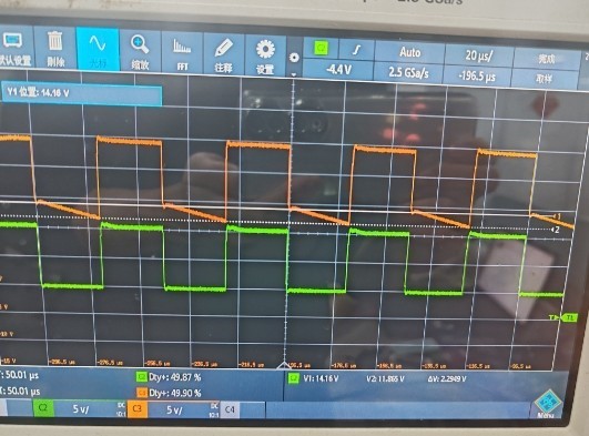
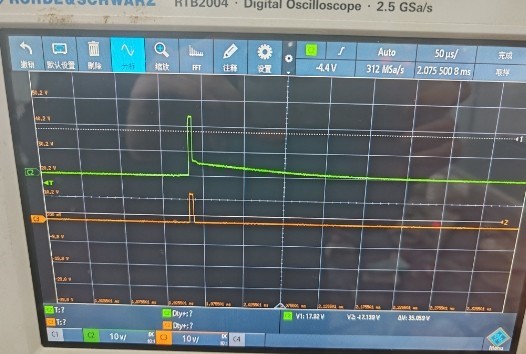
During the current product debugging process, the waveform of GH1 to GND is abnormal. The waveform is shown in the following figure. The GH1 waveform obviously shows a downward slope when the PWM is turned off, which is quite different from that of GH2.
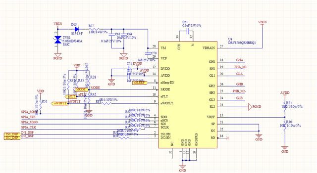
Driver configuration information: MODE is high-impedance state, controlled by PWM mode; Among the five sets of simultaneous surface mount devices, the two currently under debugging both have the same issue with the GH1 waveform.
Waveforms of GH1 and GL2 to GND:
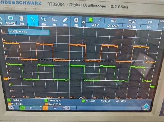
Waveforms of GH2 and GL1 to GND:
Waveform of GH1 when the external connection is disconnected
What's the reason for this?

 Channel 2 is the GH1 waveform, while Channel 3 is the waveform given by the mcu to the pre-drive. The descent is slowly turned off, but gh2 is directly turned off