DRV8834:MSP low-power microcontroller forum DRV8834:+ MPS430G2231 nENBL & nSleep pin

Part Number: DRV8834
Other Parts Discussed in Thread: MSP430G2231, MSP430WARE,

Tool/software:

I am currently using the DRV8834+MSP430G2231 combination to achieve motor control

According to the specification, drv8834 provides two motor drive modes, and I use the indexer mode.

My motor can rotate normally, but I cannot make it move forward with just one pulse. I need to send multiple steps at once to make the motor move.

I looked up the datasheet again and found that it was because I was using the nsleep pin to prevent the motor from overheating.

However, the drv8834 will return the drive coil to home when it comes out of sleep mode.

This is why it won't rotate when I send only one pulse at a time, because it keeps driving the coil in the same position.

So I try to using the nENBL pin to control my motor output
to prevent from overheating.
I followed the specifications and connected nsleep to VM and added a 47K resistor. But strangely, if I don't drive the nsleep pin low->hi once before the starts motor control , it won't turn. 
That's the line in While(1) under my main:
P1OUT &= ~BIT5;
If I mark it out, the motor becomes uncontrollable again. What's the reason?

Here is my source code, thank you.

//------------------pulse------------------
/* --COPYRIGHT--,BSD_EX
 * Copyright (c) 2012, Texas Instruments Incorporated
 * All rights reserved.
 *
 * Redistribution and use in source and binary forms, with or without
 * modification, are permitted provided that the following conditions
 * are met:
 *
 * *  Redistributions of source code must retain the above copyright
 *    notice, this list of conditions and the following disclaimer.
 *
 * *  Redistributions in binary form must reproduce the above copyright
 *    notice, this list of conditions and the following disclaimer in the
 *    documentation and/or other materials provided with the distribution.
 *
 * *  Neither the name of Texas Instruments Incorporated nor the names of
 *    its contributors may be used to endorse or promote products derived
 *    from this software without specific prior written permission.
 *
 * THIS SOFTWARE IS PROVIDED BY THE COPYRIGHT HOLDERS AND CONTRIBUTORS "AS IS"
 * AND ANY EXPRESS OR IMPLIED WARRANTIES, INCLUDING, BUT NOT LIMITED TO,
 * THE IMPLIED WARRANTIES OF MERCHANTABILITY AND FITNESS FOR A PARTICULAR
 * PURPOSE ARE DISCLAIMED. IN NO EVENT SHALL THE COPYRIGHT OWNER OR
 * CONTRIBUTORS BE LIABLE FOR ANY DIRECT, INDIRECT, INCIDENTAL, SPECIAL,
 * EXEMPLARY, OR CONSEQUENTIAL DAMAGES (INCLUDING, BUT NOT LIMITED TO,
 * PROCUREMENT OF SUBSTITUTE GOODS OR SERVICES; LOSS OF USE, DATA, OR PROFITS;
 * OR BUSINESS INTERRUPTION) HOWEVER CAUSED AND ON ANY THEORY OF LIABILITY,
 * WHETHER IN CONTRACT, STRICT LIABILITY, OR TORT (INCLUDING NEGLIGENCE OR
 * OTHERWISE) ARISING IN ANY WAY OUT OF THE USE OF THIS SOFTWARE,
 * EVEN IF ADVISED OF THE POSSIBILITY OF SUCH DAMAGE.
 *
 *******************************************************************************
 *
 *                       MSP430 CODE EXAMPLE DISCLAIMER
 *
 * MSP430 code examples are self-contained low-level programs that typically
 * demonstrate a single peripheral function or device feature in a highly
 * concise manner. For this the code may rely on the device's power-on default
 * register values and settings such as the clock configuration and care must
 * be taken when combining code from several examples to avoid potential side
 * effects. Also see www.ti.com/grace for a GUI- and www.ti.com/msp430ware
 * for an API functional library-approach to peripheral configuration.
 *
 * --/COPYRIGHT--*/
//******************************************************************************
//  MSP430G2x21/G2x31 - I2C Slave Receiver / Slave Transmitter, multiple bytes
//
//  Description: I2C Master communicates with I2C Slave using
//  the USI. Master data should increment from 0x55 with each transmitted byte.
//  ACLK = n/a, MCLK = SMCLK = Calibrated 1MHz
//
//  ***THIS IS THE SLAVE CODE***
//
//                  Slave                      Master
//                                    (msp430g2x21_usi_12.c)
//            MSP430G2x21/G2x31          MSP430G2x21/G2x31
//             -----------------          -----------------
//         /|\|              XIN|-    /|\|              XIN|-
//          | |                 |      | |                 |
//          --|RST          XOUT|-     --|RST          XOUT|-
//            |                 |        |                 |
//      LED <-|P1.0             |        |                 |
//            |                 |        |             P1.0|-> LED
//            |         SDA/P1.7|------->|P1.6/SDA         |
//            |         SCL/P1.6|<-------|P1.7/SCL         |
//
//  Note: internal pull-ups are used in this example for SDA & SCL
//
//  D. Dang
//  Texas Instruments Inc.
//  October 2010
//  Built with CCS Version 4.2.0 and IAR Embedded Workbench Version: 5.10
//******************************************************************************

#include <msp430.h>
#include <stdbool.h>
#include <stdint.h>
#define Number_of_Bytes  3                  // **** How many bytes?? ****
#define Status 0x11
#define StepH 0x22
#define StepL 0x23
#define Up 0x33
#define Down 0x34
void Setup_USI_Slave(void);
char motor_status=0;
char motor_stepH=0;
char motor_stepL=0;
char motor_up=0;
char motor_down=0;
char SLV_Addr = 0x90;                       // Address is 0x48<<1 for R/W
int I2C_State=0, Bytecount=0, transmit = 0;     // State variables
char Reg_ptr  = 0x00;                       // current reg.
bool First_wr_reg=0;                        // First write.
void Data_RX(void);
void TX_Data(void);
uint16_t adc_value = 0;
uint16_t morto_target=0;
uint8_t step;
uint8_t pre_step=0;
bool Motor_dir=0;
bool motor_active=0;
bool pi_staus=0;
bool Read_pi_state(void) { return (P1IN & BIT4) != 0; }
bool Read_DIR_state(void) { return (P1IN & BIT1) != 0; }
void Motor_Control(bool Motor_dir)
{
  if(motor_active)
  {
    P1OUT |= BIT5;
    __delay_cycles(1000);
    P2OUT &= ~BIT7; // nENBL = LOW
   
   // P1OUT |= BIT5;


    uint8_t i=0;
    if(Motor_dir)
    {
       P1OUT |= BIT1;
       __delay_cycles(100);
       
      for(i=0;i<motor_down;i++)
     {  
        P1OUT |= BIT0;            // STEP = HIGH
        __delay_cycles(250);
        P1OUT &= ~BIT0;           // STEP = LOW
        __delay_cycles(250);     //5ms = 5000 cycles @ 1MHz
      }
    }
    else
    {
      P1OUT &= ~BIT1;
      __delay_cycles(100);
      for(i=0;i<motor_up;i++)
     {  
        P1OUT |= BIT0;            // STEP = HIGH
        __delay_cycles(250);
        P1OUT &= ~BIT0;           // STEP = LOW
        __delay_cycles(250);     // 5ms = 5000 cycles @ 1MHz
      }
    }
  }
  motor_active=0;
  P2OUT |= BIT7; // nENBL = LOW (

}
static void Init_motor(void)
{
// STEP = P1.0
// DIR = P1.1
// M0  = P1.2
// sleep  = P1.5
// M1  = P2.6
// nENBL = P2.7
   
    P1DIR |= BIT0 | BIT1 | BIT2 | BIT5; // Set: P1.0 (STEP), P1.1 (DIR), P1.2 (M0) = output
    P1OUT |= BIT5;//sleep hi 1ms
    __delay_cycles(1000);
    P1DIR &= ~BIT4;      //  P1.4= input
    P1REN |= BIT4;       // internal resistor
    P1OUT |= BIT4;       // pull up
    P2SEL &= ~(BIT6 | BIT7);
    P2DIR &= ~BIT6 | BIT7;// set: P2.6 (M1), P2.7 (nENBL) output
   

    //P1OUT |= BIT5;//sleep hi 1ms
    P1OUT |= BIT1; // DIR
    P1OUT &= ~BIT2; // M0
    P2OUT &= ~BIT6; // M1
    P2OUT &= ~BIT7; // nENBL = LOW

}
void ADC_Init(void) {
    ADC10CTL0 = ADC10SHT_3 | ADC10ON;     // SHT=64 cycles, ADC10
    ADC10CTL1 = INCH_3 | ADC10SSEL_3;     // channel A3,clock:SMCLK
    ADC10AE0  = BIT3;                     // enable P1.3
}
uint16_t Read_ADC(void) {
    ADC10CTL0 |= ENC + ADC10SC;      // start trans
    while (ADC10CTL1 & ADC10BUSY);   // wait
    return ADC10MEM;                 // return value
}
int main(void)
{
  WDTCTL = WDTPW + WDTHOLD;                 // Stop watchdog
  if (CALBC1_1MHZ==0xFF)          // If calibration constants erased
  {                    
    while(1);                               // do not load, trap CPU!!  
  }
  DCOCTL = 0;                               // Select lowest DCOx and MODx settings
  BCSCTL1 = CALBC1_1MHZ;                    // Set DCO
  DCOCTL = CALDCO_1MHZ;
 
  Setup_USI_Slave();
  Init_motor();
  P1DIR &= ~BIT3;
 
  ADC_Init();
  Read_ADC();
   __delay_cycles(10000);
  adc_value = Read_ADC();
  motor_stepH=(uint8_t)((adc_value>>8)&0xFF);
  motor_stepL=(uint8_t)(adc_value&0xFF);
    __delay_cycles(1000);
      while (1)
    {
        adc_value = Read_ADC();    
        Motor_Control(Motor_dir);
        P1OUT &= ~BIT5;
        motor_stepH=(uint8_t)((adc_value>>8)&0xFF);
        motor_stepL=(uint8_t)(adc_value&0xFF);
        pi_staus=Read_DIR_state();
        //P2OUT |= BIT7; // nENBL = LOW
    }
  //LPM0;                                     // CPU off, await USI interrupt
  //__no_operation();
}

//******************************************************************************
// USI interrupt service routine
// Rx bytes from master: State 2->4->6->8
// Tx bytes to Master: State 2->4->10->12->14
//******************************************************************************
#if defined(__TI_COMPILER_VERSION__) || defined(__IAR_SYSTEMS_ICC__)
#pragma vector = USI_VECTOR
__interrupt void USI_TXRX (void)
#elif defined(__GNUC__)
void __attribute__ ((interrupt(USI_VECTOR))) USI_TXRX (void)
#else
#error Compiler not supported!
#endif
{
  if (USICTL1 & USISTTIFG)                  // Start entry?
  {
    I2C_State = 2;                          // Enter 1st state on start
    USICTL0 &= ~USIOE;
  }

  switch(__even_in_range(I2C_State,14))
    {
      case 0:  USICTL0 &= ~USIOE;                              // Idle, should not get here
              break;

      case 2: // RX Address
              USICNT = (USICNT & 0xE0) + 0x08; // Bit counter = 8, RX address
              USICTL1 &= ~USISTTIFG;        // Clear start flag
              I2C_State = 4;                // Go to next state: check address
              break;

      case 4: // Process Address and send (N)Ack
              if (USISRL == 0x91){            // If master read...
                SLV_Addr = 0x91;             // Save R/W bit
                transmit = 1;}
              else if (USISRL == 0x90)
                {transmit = 0;
                SLV_Addr = 0x90;}
              USICTL0 |= USIOE;             // SDA = output
              if (USISRL == SLV_Addr)       // Address match?
              {
                USISRL = 0x00;              // Send Ack
                if (transmit == 0){
                  First_wr_reg=1;             //to get current
                  I2C_State = 6;}           // Go to next state: RX data
                if (transmit == 1){  
                  First_wr_reg=1;             //to get current
                  I2C_State = 10;}          // Else go to next state: TX data
                  USICNT |= 0x01;               // Bit counter = 1, send (N)Ack bit
              }
              else
              {
                USISRL = 0xFF;              // Send NAck
                I2C_State = 0;              // next state: prep for next Start
                Bytecount =0;                 // Reset counter for next TX/RX
               
              }
              USICNT |= 0x01;
              break;

    case 6: // Receive data byte
              Data_RX();
              break;  

      case 8:// Check Data & TX (N)Ack
              USICTL0 |= USIOE;             // SDA = output
              if(First_wr_reg)
              {
              Reg_ptr=USISRL;
              First_wr_reg=0;
              }
              else
              {
               switch(Reg_ptr)
               {
                  case Status:motor_status = USISRL;break;
                  case StepH:
                        motor_stepH  = USISRL;
                        morto_target = (morto_target & 0x00FF) | ((uint16_t)motor_stepH << 8);
                        break;
                  case StepL:
                        motor_stepL  = USISRL;
                        morto_target = (morto_target & 0xFF00) | StepL;
                        break;
                  case Up:
                        motor_up     = USISRL;
                        motor_active=1;
                        Motor_dir=0;//go adc ++
                        break;
                  case Down:
                        motor_down   = USISRL;
                        motor_active=1;
                        Motor_dir=1;//go adc--
                        break;
               }
              }
              if (Bytecount <= (Number_of_Bytes-2))          
                                            // If not last byte
              {
                USISRL = 0x00;              // Send Ack
                I2C_State = 6;              // Rcv another byte
                Bytecount++;
                USICNT |= 0x01;             // Bit counter = 1, send (N)Ack bit
              }
              else                          // Last Byte
              {
                USISRL = 0xFF;              // Send NAck
              USICTL0 &= ~USIOE;            // SDA = input
              SLV_Addr = 0x90;              // Reset slave address
              I2C_State = 0;                // Reset state machine
              Bytecount =0;                 // Reset counter for next TX/RX
              }
             
             
              break;

     case 10: // Send Data byte
              TX_Data();
              break;

      case 12:// Receive Data (N)Ack
              USICTL0 &= ~USIOE;            // SDA = input
              USICNT |= 0x01;               // Bit counter = 1, receive (N)Ack
              I2C_State = 14;               // Go to next state: check (N)Ack
              break;

      case 14:// Process Data Ack/NAck
           if (USISRL & 0x01)               // If Nack received...
              {
              USICTL0 &= ~USIOE;            // SDA = input
              SLV_Addr = 0x90;              // Reset slave address
              I2C_State = 0;                // Reset state machine
               Bytecount = 0;
             // LPM0_EXIT;                  // Exit active for next transfer
              }
              else                          // Ack received
              {
                TX_Data();                  // TX next byte
               }
         break;
   
      }
  USICTL1 &= ~USIIFG;                       // Clear pending flags
}

void Data_RX(void){
 
              USICTL0 &= ~USIOE;            // SDA = input
              USICNT |=  0x08;              // Bit counter = 8, RX data
              I2C_State = 8;                // next state: Test data and (N)Ack
}

void TX_Data(void){
                   switch(Reg_ptr)
               {
                  case Status:USISRL=motor_status;break;
                  case StepH:USISRL=motor_stepH ;break;
                  case StepL:USISRL=motor_stepL ;break;
                  case Up:USISRL=motor_up ;break;
                  case Down:USISRL=motor_down ;break;
                  default:
                  USISRL=0xFF;break;
               }
              USICTL0 |= USIOE;             // SDA = output
             // USISRL = SLV_Data++;
              USICNT |=  0x08;              // Bit counter = 8, TX data
              I2C_State = 12;               // Go to next state: receive (N)Ack
}

void Setup_USI_Slave(void){
  P1OUT = 0xC0;                             // P1.6 & P1.7 Pullups
  P1REN |= 0xC0;                            // P1.6 & P1.7 Pullups
  //P1DIR = 0xFF;                             // Unused pins as outputs
  P2OUT = 0;
  P2DIR = 0xFF;
 
  USICTL0 = USIPE6+USIPE7+USISWRST;         // Port & USI mode setup
  USICTL1 = USII2C+USIIE+USISTTIE;          // Enable I2C mode & USI interrupts
  USICKCTL = USICKPL;                       // Setup clock polarity
  USICNT |= USIIFGCC;                       // Disable automatic clear control
  USICTL0 &= ~USISWRST;                     // Enable USI
  USICTL1 &= ~USIIFG;                       // Clear pending flag
 
  transmit = 0;
  __enable_interrupt();

}
 
  • HI Tseng, 

    Thank you for your question. 

    The nSleep pin is utilized to place the driver in sleep mode, where a logic high enables the device and a logic low initiates low-power sleep mode, resetting all internal logic. To bypass sleep mode, the nSleep pin can be pulled up to VM through a 47kΩ resistor, and the output can be enabled using the nENB pin. Following power-up, the device is ready to control the output by applying logic low to the nENBL pin, with the home state defaulting to 45°. This state is entered after power-up, undervoltage lockout exit, or sleep mode exit. By applying a step pulse, the motor can be stepped forward.

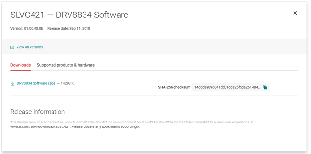
    For your reference, a firmware written for the DRV8834EVm evaluation module using the MSP430 microcontroller is available below.

    DRV8834EVM Evaluation board | TI.com

    Best regards, 

    Mojtaba