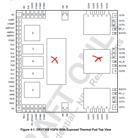
DRV7308: Connection point location for thermal performance testing

Part Number: DRV7308


Tool/software:

Hello team,

I had a quick question on the connection point location for thermal testing,

Could you please share the x,y axis points of the connection point (or test/tapping point) for the IC, for thermal performance test?

Customer asked the exact point where the IC would be heated up the most, so they can connect their wire on that exact point for their thermal performance testing. 

Thank you.

  • Hi Jade,

    A thermal camera is helpful to identify the exact point for the customer's specific PCB for the hottest point for thermal heating, however oftentimes this will be above OUTB due to PCB copper area being oftentimes more restricted for phase B compared to A and C. If there is poor PGND area, then it is possible that the low side will get the hottest. The below two points on the package will likely be approximately the hottest points depending on the layout.

    Regards,

    Anthony Lodi

  • Hi Anthony,

    Thank you so much for your detailed feedback!

    I had a follow-up question from customer,

    If so, where is the IC integrated temp sensor located, and therefore which block's temperature does the temp sensor measure & show?

    Usually with their previous IPMs the integrated temp sensors measured Tc point (case temp point), where the temperature is the highest on the case. Therefore, they must have the IPM temp sensor's data to match the measurement data of thermal performance test (via connection point) completely.

    Customer requested a detailed & accurate explanation on this, like you have kindly shared, because this is important for them. Could you please share your feedback on this topic? 

    Thank you for your help and support.

    Best regards,
    Jade

  • Hi Jade,

    Let me look into this more and provide a response hopefully by the end of the week.

    Regards,

    Anthony Lodi

  • Hi Jade,

    The temp sensor is located on the low side driver in the DRV7308. I will work to get you an approximate location of where it is located on the package. What we have seen based on thermal simulations (assuming 0.35W of power dissipation in each FET) that the temperature difference between the hottest point on the high side GaN and the temp sensor was 10C hotter at the GaN compared to the temp sensor temperature.

    with their previous IPMs the integrated temp sensors measured Tc point (case temp point), where the temperature is the highest on the case.

    We looked into this and it seems that actually the Tc point is not referring to where the temp sensor is located, but rather is the point on the device at which the Theta JC was calculated. 

    Regards,

    Anthony Lodi