DRV8908-Q1: DRV8908-Q1 EMC failure with ISO11452-2 (Bulk current injection)

Part Number: DRV8908-Q1


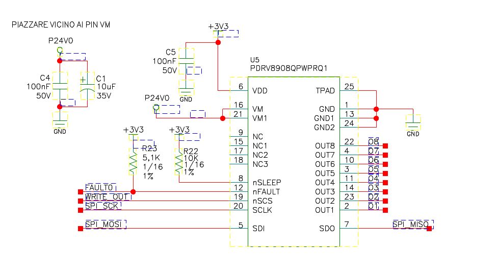
Good morning. We are using the DRV8908QPWPRQ1 integrated circuit to drive various types of output loads. In our case, we are driving a 5mA load connected to ground with a 1Hz square wave. The VM voltage supplied to the integrated circuit is 24V.
In the ECER10 ISO11452-2, 20-200MHz, 60mA (AM 1KHz 80%) Bulk Current Injection test, we are experiencing output failures. During the test, the output subjected to interference randomly locks up, either at a high or low logic level. When the interference is removed, the output resumes functioning correctly.
The interference frequency at which the problem occurs is around 70MHz.
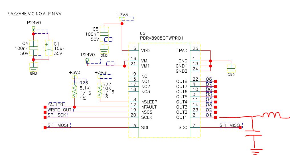
We tried placing a 10nF capacitor on the DRV8908 output, but it is not sufficient.
We also added a ferrite bead (Murata BLM31PG601SN1) in series with the output, in addition to the capacitor, but while it improved, the problem shifted in frequency and persisted.
What can we do to pass the test?
What's happening in the integrated circuit?
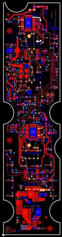
We've attached the original wiring diagram and the one with the tested modification.

Best regards

MauroDRV8908_Original.JPGDRV8908_Modified.JPG

  • Hi Mauro,

    I will have to reach out to our EMC expert on this issue. I will aim to provide an update on Wednesday.

    Regards,

    Joshua 

  • Hi Joshua.

    We forgot an important piece of information. The Bulk Current Injection test is performed on the wire of the single output connected to the load, as the load is external to the board and can be several meters away. The test is then repeated for each output on the board.
    Thank you for your support.

    Regards

    Fabio

  • Hi All,

    I do not have experience with DRV8908 but I would check the following:

    - is nFAULT output active when problem occurs?

    - does SPI communication work when problem occurs?

    PCB layout:

    - is there a ground layer present under whole circuit?

    - placement and connection of VM and VDD decoupling capacitors (parasitic inductances),

    - possible coupling between output traces and SPI traces,

    - placement and connection of added filter capacitors (parasitic inductances).

    Regards,

    Grzegorz

  • Hi Gregorz

    Below my answers:

    - is nFAULT output active when problem occurs? No, the fault signal is not acrivated 

    - does SPI communication work when problem occurs? Yes

    PCB layout:

    - is there a ground layer present under whole circuit? Yes

    - placement and connection of VM and VDD decoupling capacitors (parasitic inductances)

    - possible coupling between output traces and SPI traces,             

    - placement and connection of added filter capacitors (parasitic inductances).

    We have tried to follow all the instruction about layout and circuit reported on the  datasheet.

    What kind of problem could have the DRV on the output side?

    Regards

    Mauro

  • Hi Mauro,

    From our testing and analysis, the frequency injected into the output pin will affect the pull-up current source on the HS gate preventing the MOSFET which will prevent the HS MOSFET from opening or closing.

    A solution that could be used would be to add a low pass filter onto the output targeting the frequency where the failures begin.

    Regards,

    Joshua

  • Hi Jousha,
    In the bulk current test, our board's current output has a minimal load (about 5mA), but in reality it can reach 200mA.
    The board is very small (there are 8 or 16 outputs depending on the board version), so it's difficult to insert low-pass filters, consisting of a simple RC circuit (due to the power dissipated by the resistor, which, although small in value, e.g., 10 ohms with 1nF, dissipates quite a bit at maximum load).
    We could compose an inductive low-pass filter; it might be more manageable, although I fear the available space isn't sufficient.
    Could simply increasing the value of the output capacitor (up to a few microfarads) help?
    Any other ideas?
    We'll be back in the lab soon for further precompliance tests, and we'd love to have some good "cartridges" to fire!
    We'll also test the filter solution on a single output, though it will be difficult to apply it to all outputs on the current board.

    Thanks for your help.

    Have a nice day.

    Fabio

  • Hi Fabio,

    - 200 mA output current would well suit ferrite bead like the one you used, it should have nominal current at least 5 times higher ie. 1A (ferrite core saturation

    makes ferrite beads less effective).

    - For MLCC cap selection you can use Murata SimSurfing online tool https://ds.murata.com/simsurfing/index.html?lcid=en-us, for 20-200MHz I would try

    something like 100nF, 0603 MLCC cap. Larger caps like 0805 etc. have larger parasitic inductance,

    - I would focus on good PCB layout, at 100-200 MHz every millimeter of trace and nanohenry of parasitic inductance starts to have an impact,

    - With good PCB layout maybe single capacitor + ferrite bead would be enough and more complex filters like Pi or T will not be needed,

    - It would be worth trying to place ferrite bead first from DRV side.

    - If you can share PCB area around DRV and output filter I can try to help with PCB layout.

    Regards,

    Grzegorz

  • Hi Grzegorz
    I'm sending you some images of the board layout.
    The path to output number 1 is highlighted in white in the images.
    This board can have up to 16 outputs divided into two DRVs.

    Regards

    Mauro

  • Hi Mauro,

    Thank you for sharing all the above information. 

    Can you tell:

    - What was cable length during EMC test and distance between PCB board and device injecting HF current (I guess HF current probe)?

    - Was current injected into single wire or the whole cable?

    - Is PCB board a 4-layer one with two inner layers as ground planes?

    A few things that I would do according to Layout Example Fig 163 in DRV8908-Q1 datasheet:

    - thicker GND pads/traces on DRV8908 or even solid ground as it is on Fig 163 (cons - more difficult rework),

    - one decoupling MLCC cap 100nF for every VM pin, these caps should be on the same board side as DRV,

    - C5 cap should also be on the same side as DRV as well,

    - possible short and thick traces between above mentioned caps and DRV pins, two ground vias for every capacitor gnd pad close to gnd pad,

    Other suggestions:

    - I would place as many components as possible on the same side as DRVs, it would give more space for possible output filters. During HF current injection the cable will radiate EMI and it is better to keep it away from as many components and traces as possible.

    - I would place more ground stiching vias across the board,

    - it is a good practice to place also ground vias close to places where traces change layers from top to bottom and vice versa.

    I noticed dark yellow pads on connector that are probably power supply, I would place at least one MLCC 100nF decoupling cap close to each connector end where those pads are connected to traces going to other components.

    Low pass output filters, if I have enough space I would add footprints for Pi filters, two MLCC caps 0603 and one ferrite bead 0805. One cap should be placed possible close to the connector and other one to DRV. If there is not enough space probably I would eliminate DRV cap. I would use 100nF for a single cap filter or 2x47nF for Pi filter. For a ferrite bead probably I would choose 1,5A 1kOhm like MFBM1V2012-102-R. Ground plane under connector area should be solid, capacitors ground pads should be connected to ground plane with two vias if possible. During EMC tests if other DRV outputs are connected to the cable all filters should be present on board.

    Regards,

    Grzegorz

  • Hi Grzegorz

    Below my answers:

    - what was cable length during EMC test and distance between PCB board and device injecting HF current (I guess HF current probe)? MB:  Cable length was 2m, distance from device injecting HF current was 0,2m (like the standard requires)  

    - Was current injected into single wire or the whole cable? MB:  we have tried both but expecially with a single wire

    - Is PCB board a 4-layer one with two inner layers as ground planes? MB:  4 layer but only one is the GND Planes, the other is for 3V3 and 24V

    - thicker GND pads/traces on DRV8908 or even solid ground as it is on Fig 163 (cons - more difficult rework): MB The thermal pad is connected to ground plane with a lot of vias.

    Thank you for the suggestions.

    Today we need help to obtain the compliance with the standard and solve the problems using the actual PCB manually modified.

    The PCB it is quite thight and full of components, for the future will be better for us try to use one capacitor.

    Best regards

    Mauro

  • Hi Mauro,

    Thank you for your answers.

    "Cable length was 2m" - it would be around 1/2 of wavelength for 70MHz, if problem occurs only at 70 MHz or 140MHz then cable length may play a role. Just my guess.

    "only one is the GND Planes, the other is for 3V3 and 24V" - that makes design of PCB for EMC more difficult.

    "we have tried both but expecially with a single wire" - if problem occurs mainly with single wire then differential mode is the problem and you may try to solder a few MLCC caps 100nF between output pads and GND pads of the connector, plus between VM pads and GND pads of the connector.

    I think that now EMI may affect DRV through:

    - output lines directly,

    - output lines and DRV output Mosfets into DRV VM line,

    - VM connector lines into DRV VM pads which are not very well decoupled.

    I am going now on my short holiday, I should be back at end of the next week.

    Best Regards,

    Grzegorz