This thread has been locked.

If you have a related question, please click the "Ask a related question" button in the top right corner. The newly created question will be automatically linked to this question.

Fault and Warning Reporting and Handling in DRV8302

Other Parts Discussed in Thread: INSTASPIN-BLDC, CONTROLSUITE

Dear All,

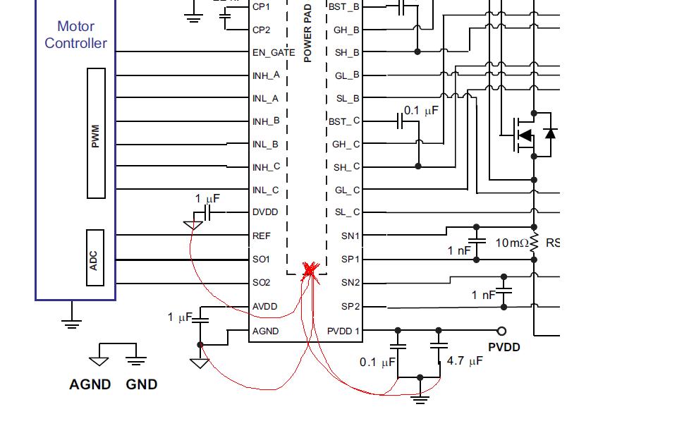
 I am debugging using customer board(TMS320F28035 + DRV8302: DC bus voltage: Max 32V, Phase Current: Max 20A, RPM: Max 3000RPM, PWM= 15kHz, Servo Motor).

Unfortunately we found "FAULT" signal as soon as we operated.

(The signal pattern of "FAULT" pin is " High-Low-High-Low-High-Low-...". As it were, high-low pattern repeated continuously.)

So we checked all spec sheet of DRV8302.

-. 10ms delay is right after setting EN_GATE.

-. We could not found out any "Fault and Warnging Reporting and Handling" at page 15 of DRV8302 spec sheet.

   (PVDD Undervoltage, DVDD undervoltage, GVDD undervoltage, OTW, OTSD_GATE, OTSD_BUCK, Buck Output undervoltage, Buck Overload,

 External FET overload-current limit mode, External FET overload-Latch mode, External FET overload-reporting only mode)

How can we solving this error?


Please help me.

Sincerely,

Joseph

  • Which SW are you using (does the InstaSPIN-BLDC GUI connect and show a green button?), or is the fault on immediately?

    How is the solder joint on the CAP between the PWR and GND connectors?

  • Thank you Chris!

    The board is customer board.

    (customer designed SW based on  /ControlSuITE/device_support/f2803x.)

    The connections of CAP between PWR and Ground are good.


  • Joseph,

    My best guess with the information provided is to check the GND connections on the decoupling for AVDD (pin 28), DVDD (23), and PVDD1 (29).  The GND connections for these decoupling capacitors need to be as close as possible to the PowerPAD GND connection (the exposed pad on the bottom of the IC).  

    Also note, the PowerPAD must be soldered to the PCB and have a solid connection to board GND.  This is the only GND connection for the IC and must be made for proper functionality.  

    I have attached a visual of how this should be done.  The traces need to be as short as possible.