This thread has been locked.

If you have a related question, please click the "Ask a related question" button in the top right corner. The newly created question will be automatically linked to this question.

DRV8703-Q1: Chip burns out

Part Number: DRV8703-Q1

Hello!

I'm having a problem: the chip keeps failing—either immediately or after a while. The chip driver is connected to the motor via MOSFET transistors, but the motor isn't running, so the driver isn't being controlled. The 24V line is protected by a TVS diode.  The resistors  R1, R7 and R8 then get very hot and fail.   The chip itself then shorts out on almost all of its pins. The Mosfets transistors are ok, don't fail. We have two grounds, G and PG, which are shorted at a single point. The chip often fails when connected to a 24V battery. Last time, we powered it from a power supply, and it later simply failed on its own without being used. Help!
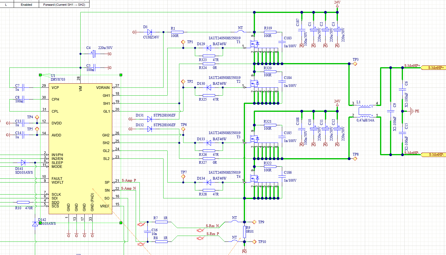
  Screenshot 2026-02-05 142717.png

  • Hi Stanislav, 

    Thank  you for your question. Please help me to understand the situation better through following questions. 

    1- Is this a new design or old? is the schematic reviewed by TI?

    2- When this issue is started and was there any changes in the device that results in this issue?

    3- Regarding the schematic, would you please let me know:

       a: What is L1 and why it is being use? 

       b: What is the motor output current?

       c: why D129-130  and D133b, 134 are used? 

       d: What is the reason for R1: 100 ohm, R7, R8 and also C16? 

       e: What is the reason for using D141, and D142.

       f: are the WDFLT and FAULT pins pulled up?

    4- 

    The chip driver is connected to the motor via MOSFET transistors, but the motor isn't running, so the driver isn't being controlled. The 24V line is protected by a TVS diode.  The resistors  R1, R7 and R8 then get very hot and fail.

    The R7 and R8 resistors are connected to the SN,SP pin. I do not understand why they are getting hot? Please capture the voltage across the SN, and SP pin. 

    5- 

    The chip often fails when connected to a 24V battery. Last time, we powered it from a power supply, and it later simply failed on its own without being used

    It seems that it is abs max violation. Please capture the SH1,SH2, SL2 and Drain pin waveform when the failure happens. 

    Best 

    Mojtaba

  • Hello Motjaba!

    Thank you for your quick reply! 

    Honestly, this isn't my design, but I'll try to answer the questions.

    1. This is a new circuit and has never worked.

    3.

    a: L1 is to reduce interference on wires to motor.

    b: Output current is 15A, peak 25A.

    c: D129-130 may be to pull the gate to ground faster; D133b and 134 - no idea.

    d: R1 is to limit current in case of a fault; R7, R8, and C16 are low-pass filters for the amplification signal.

    e: D141 and D142 are the logic circuit to turn off the chip from multiple sources - putting it into sleep mode.

    f: Are the WDFLT and FAULT pins pulled up? Yes

    4- The R7 and R8 resistors are connected to the SN and SP pins. If the chip has a short circuit, there is 24V at the SP and SN pins.

    5- Yes, I can do that. The fault often occurs immediately after switching on, without the motor being activated.

    So, if you mean we must make any changes in the design, we will test it!

  • Hi Stanislav, 

    . This is a new circuit and has never worked.
    The R7 and R8 resistors are connected to the SN and SP pins. If the chip has a short circuit, there is 24V at the SP and SN pins.

    There is no internal path from 24V to SP/SN. and also, I do not see external path. It seems that there is abs max violation on the Power or output pins which resulted in internal short circuit.  To find out the root cause, we need to check the voltage on pins. Please measure the requested waveform to have a better understanding. 

    There are some changes that Would like to be applied based on the points noted above, But for now we need to find out the reason behind device failure. 

    During your test, please remove the L1 and see if the device still see failure. 

    Best

    Mojtaba

  • Hi Mojtaba,

    I'm continuing to work on the design and have taken a series of measurements.
    We captured the following waveforms: GH1, GL1, SH1, DVDD, AVDD, GH2, GL2, SH2, SP, SL2, and SN.

    Measurements were performed during system startup, idle operation, and while the motor was running.
    In the first test run, we used the design as-is. In a second run, we removed L1 to see whether this introduced any noticeable differences.

    Based on the data so far, none of the signals violate the absolute maximum ratings and everything remains within specification.
    The error has not reappeared, and at this point we don’t have a reliable way to reproduce it. Even stress‑testing the board with repeated power cycles and various motor movements hasn’t triggered a failure.

    Issues like this are difficult to isolate, but if you have additional ideas or diagnostic steps we could try, we’d be happy to explore them.

    Best regards,
    Alexander Miller
  • Hi Alexander, 

    Thank you for your measurements.

    Under what condition, did you measure the test points? Both GH1 and GL1 are at their high condition and it means that both HSFET and LSFET are ON, and there is a shoot through form TI, T2, and R9.

    1-Please let me what are the input (IN1 , IN2) mode pins value.

    2- Please capture GH1, GL1 and SH1, IN1 waveform using oscilloscope. 

    Best 

    Mojtaba

  • Hi Mojtaba,

    the highlighted measurements were taken during motor operation (startup and running). The values shown represent only the maximum voltages observed on each pin during the measurement window. GH1 switched to High and GL1 to Low as expected, so there is no indication of shoot‑through. 

    The previously reported high voltage on SH1 was an error on my part when creating the table. The oscilloscope originally showed a max of 26 V, but this was caused by measurement artifacts due to the long probe leads used during testing. Here is the capture with the artifacts (CH1=GH1, CH2=GL1, CH3=SH1, CH4=DVDD):
    After repeating the measurement with shorter leads, these small peaks disappeared.
    The actual SH1 voltage is approximately 21.4V (25V max), which is within specification.

    1. The driver is currently configured in PH/EN mode, and the motor is driven in only one direction at a 100% duty cycle.
    Below is a capture of IN1 (CH1) and IN2 (CH2) during motor startup:


    2. As requested, we also repeated the measurements for IN1 (CH1), GH1 (CH2), GL1 (CH3) and SH1 (CH4). Once during system startup (motor not running): 
    and once during motor startup:


    If you would like, we can provide separate screenshots for each signal to give a more detailed view.
    Best regards
    Alexander Miller
  • Hi Alexandra, 

    The previously reported high voltage on SH1 was an error on my part when creating the table. The oscilloscope originally showed a max of 26 V, but this was caused by measurement artifacts due to the long probe leads used during testing. Here is the capture with the artifacts (CH1=GH1, CH2=GL1, CH3=SH1, CH4=DVDD):

    Are the highlighted in the figure1 below due to measurement artifact? In the last screen shot figure 2, this glitch can be seen. 

    The other screenshots looks ok. are they with L1? 

    have you been able to repeat the failure and capture the screenshots.?

    Have you tried PWMing the IN1 input and see if you can replicate the failure?

    It is needed to first find the condition that the device is getting failed and then capture the waveforms. 

    Figure 1:                                                                                                  Figure 2


    If the glitches above are due to the measurement, as you mentioned " The resistors R1, R7 and R8 then get very hot and fail." 

    Max current is 25 A and the Rsense is 0.01 which results in 0.25V and the current onR7/R8 is in ua ranges. So to find the reason behind the high current on R1/R7/R8 it is needed to measure SP to SN, SP to GNd and SN to GND, Vdrain, and measure load current? Find the condition that the failure is replicable. 

    Also I would see NT in the path of R1/R7/R8 resistors. what are those and why thet being used. 

    Best

    Mojtaba