This thread has been locked.

If you have a related question, please click the "Ask a related question" button in the top right corner. The newly created question will be automatically linked to this question.

DRV8301: reset source for CR1 and CR2

Other Parts Discussed in Thread: DRV8301

Hi...

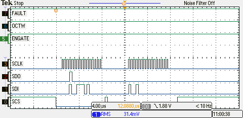
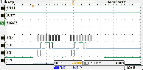
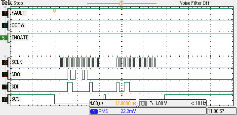
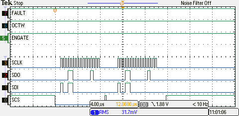
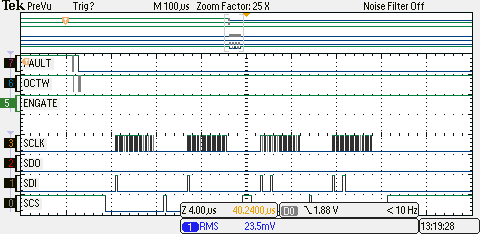
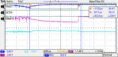
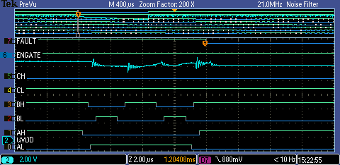
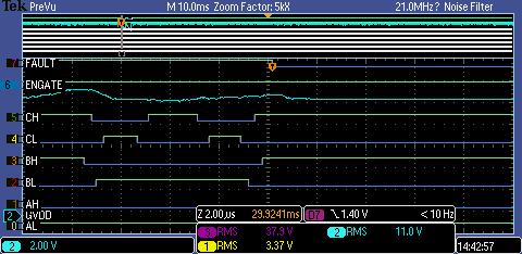
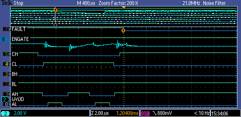
i'm using the DRV8301 in ebike project replacing 3 halve bridge drivers, op and switching regulator of the existing circuit. I'm able to configure the chip over SPI and can read back the register values. The read register values are the same which i've configured at startup - as long as the motor is not running.

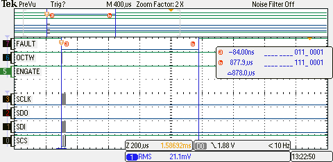
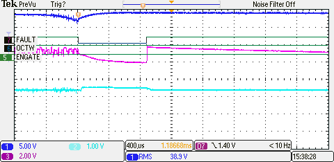
At startup of the motor (or a few seconds later) the register values CR1 and CR2 are reseted to default values.

I've checked that

a) EN_GATE is not low (could lead to quick reset (<10us) or power down (>=10us))

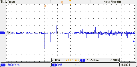
b) PVDD is valid (no spikes down to UV)

c) no spi write command to register CR1 or CR2

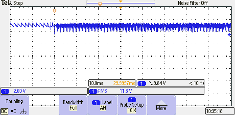
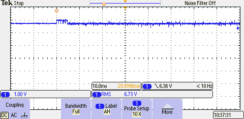
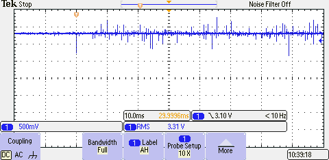
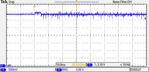
I stumpled about that problem while monitoring the output of the OP discovering that the gain factor is reset to 10.

Any ideas what could be the reason for that problem or how to track it down?

Thanks for your help

Gerd

  • Gerd,

    This is very curious.  A couple of clarifying questions:

    1)  You mentioned you did a read back after a WRITE on SPI and the gain was set as you had programmed.  What was it programmed to?  Did you verify that the gain measured on the output of the op-amp matched the read-back value?  

    2)  Is VDD_SPI (pin 49) at the same voltage as the logic-level of your SPI pins?

    3)  What PVDD are you operating at?

  • Ryan,

    i hope i can clarify your questions:

    1) I've tried a gain of 80, 40 and 20 but the last tests were made with a gain of 40. Sometimes (seldom) the registers are not reset on startup of the motor. In that case the voltage at op output is 4 times higher that with the default gain of 10. I can attach scope pictures and the register values i've programmed tomorrow (it's10:30pm here in germany) when i'm at work again.

    2)The buck converter inside the DRV8301 generates 5V and the 3.3V for VDD_SPI and cpu is generated from that 5V via a second buck converter.

    3) PVDD is 28..42V out of a lion battery but currently i'm using ca. 39V from a power supply. A 1800uF capacitor attached on PVDD is located near DRV8301.

    I attached a scope to PVDD, VDD_SPI and the voltages where ok. I measured DVDD and there was only a ~100mV ripple at startup. If needed i can attach scope pictures of voltages and spi communication.

    Gerd

  • PVDD1 38.4V startup of motor

    GVDD

    AVDD

    VDD_SPI

    DVDD

    Write of CR1

    Read of CR1 (0x03A0)

    Write of CR2

    Read of CR2 (0x0008)

    After motor startup CR1 is 0x0000 and CR2 is 0x0000

    Gerd

  • Just noticed that if iset gate driver peak current to

    1) 1.7A: CR1 and CR2 are reset

    2) 0.7A: CR1 and CR2 are not reset but at higher rpm they are

    3) 0.25A: CR1 and CR2 are not reset but at higher rpm they are

    Noticed no difference in rpm between (2) and (3)!. So it looks like a voltage problem due to high gate currents?

    Gerd

  • Starting with (3) from previous post i've made a fault interrupt routine reading out the status register 1/2:

    As you can see nothing is read back (no address bit set on SDO while read of SR2)! The whole fault duration is ~890us:

    Gerd

  • I measured PVDD (blue), GVDD (pink) and DVDD (cyan):

    Same (enlarged) with cursors on PVDD: Fault was generated at ~36.4V instead of normal voltage of 39.2V. Should be far away from uv reset.

    Gerd

  • Gerd,

    Try inserting some series resistors between the gate driver outputs and your FETs.  We have 1 ohm on our EVM, but you should try up to 10 ohm.  This would eliminate any "false" OCP trips that might be occurring due to the fast switching edges. 

  • Ryan,

    thanks for the hint - i'll try it out and report the results. Currently i'm using 4R7 between gate driver output and gate of BSB028N06 (Infineon).

    Gerd

  • Ryan,

    sorry for the long delay. I replaced (the serial gate resistor) 4R7 with 10R and after that with 15R. Now i can use the 1.7A gate driver setting but the reset still occurs with any gate driver current setting (0.25A, 0.7A, 1.7A). Do you have further suggestions for me to try?

    Thanks for your help

    Gerd

  • I did some more measurements and it looks like that the reset is triggered be a few different PWM patterns. Below one example:

    Pattern on phase A/B

    Pattern on phase B/C

    Pattern on phase A/C

    Any ideas where to focus on? Charge pump capacitor? GVDD cap? Bootstrap cap?

    Gerd

  • Gerd,

    Have we completely eliminated OC?  This can be done via the control bits in control register 1.  The series resistors seemed to help move out the trip point, so I still feel like we are getting "false" OC trips here.

  • Just 9 month later (and some other projects in between) we've done a new ("emc corrected") layout of our board.

    "emc corrected": 2 layers instead of 4, solid ground on both sides (not splitted into AGND, DGND and so on), a lot of vias (~ 5times more than before), protecting/isolating hot/shunt/spi traces with fences of vias, small loops on all switching regulators (4), integrating pi filter in front and after switching regulators.

    Now all is ok so far and i can continue with my work. If i find some other difficulties/problems i'll open a new thread.

    Gerd

  • Gerd,

    Appreciate the follow-up....glad all is well for now.