This thread has been locked.

If you have a related question, please click the "Ask a related question" button in the top right corner. The newly created question will be automatically linked to this question.

DRV8301: dead gate drive section

Other Parts Discussed in Thread: DRV8301

Hi,

I've designed a sensorless motor drive using DRV8301. I'm very satisfied by this IC, but I have a problem that I can't work out by myself.

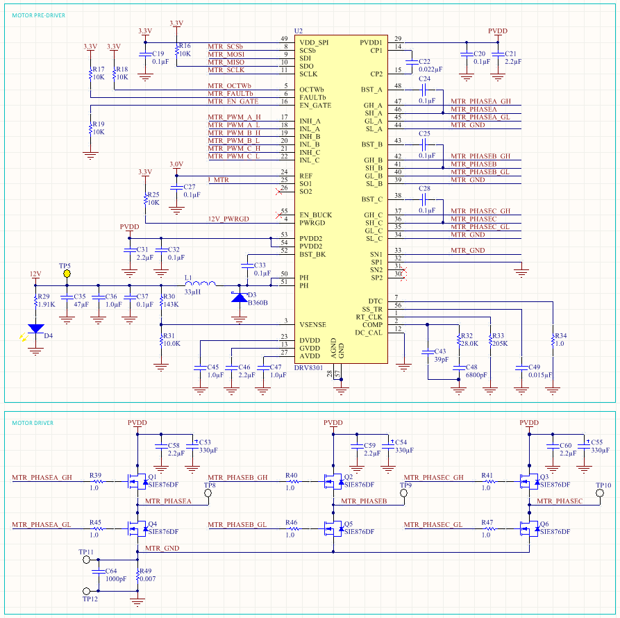
During the first tests the gate drive section has broken down after a few hours of work. The buck section is still working but the gate drive is not. All the charge pump voltages are at 0V.

My supply voltage range is 35-60V and the damage has occured at about 45V, quite distant from the absolute maximum. The board was quite warm (40°C) but nothing dangerous.

My power section is quite similar to drv8301-hc-c2-kit. The only significant difference i see is that we are using two 1uF capacitors on GVDD instead of one 2.2uF. We should still be inside +/-20% raccomended range, but I don't know exactly what could happen with the DC bias applied.

Do you have any suggestion ?

  • We have done an x-ray analysis and the PVDD1 internal track results clearly vaporized. The adjacent track is also damaged. It seems the result of an output short circuit but the system was standing on a desk when it stopped working.

  • Simone,

    Wow....the finger of the leadframe is completely taken out.  

    Something else must have gone wrong on the die that caused a lot of current drain on the PVDD track.  A difference in capacitance on GVDD would not cause something like this.  I have never actually seen a failure like this and not sure what could cause it without taking a closer look at the die.  

    Where did you get the device?  If you ordered through distribution, please return it through the distribution channel and we can do a formal failure analysis on it.  If you sampled it, you can call TI support line to return the device.  

  • Hi Ryan,

    thanks for the reply.

    The device comes from Digikey and we will try to return it as soon as we can. The problem is desoldering it without further damage since its power pad is quite "powerful".

    I'm asking myself if a similar breakdown could be caused by a subtle damage during the soldering process. What do you think?

  • Hello,

    Have there been any conclusions regarding this issue?  I have had a very similar failure mode in my design (also based very closely on the DRV8301-HC-C2-KIT development kit).  Twice I have had a board run successfully on the bench for 1-2 hours, only to have it fail.  The drivers stop functioning (but the buck regulator continues to operate) and the device gets very warm.  I am running this under very light loads: 30V at 500mA.  

    Any advice would be greatly appreciated!

    Thanks.

  • Hi Jessica,

    my problem was quite subltle. I try to summarize.

    1. There was an occasional self turn on of the lower mosfets due to very high dv/dt 
    2. In that cases a large current spike was recalled from the large li-ion battery I use in my application
    3. The mosfets survived and they turned off due to overcurrent protection
    4. Inductive kickback from the battery wiring gave me a large voltage spike in Vbus
    5. Gate driver section of DRV8301 made the role of a TVS diode and it went into smoke
    The problem was solved increasing dead time and switching to lower driver currents.
    Bye and good luck.
  • Hello Simone,

    Thank you very much for replying so quickly.

    I'm not sure that I am seeing the same problem, exactly.  I had my boards hooked up to a power supply with a fairly low current limit (3A).  I also have a large TVS diode (SM8S43A) across my power bus between my driver circuit and the pre-driver, so any spikes would hopefully be absorbed by that and not the DRV8301.

    The DRV8301 datasheet does mention a maximum supply voltage ramp rate of 50V/ms.  This seems like an odd rating to me, especially since it's not mentioned anywhere else in the datasheet or the demo examples.  Perhaps I am getting spikes on my PVDD line which are less than the breakdown voltage of my TVS but fast enough to damage the DRV8301 chip.  Still, if this were the case I would think more people would be having an issue with this device.  I think I will try putting a ferrite bead in line with the power to the DRV8301 to see if that helps.

    Your help is very much appreciated,

    Jessica

  • Thanks Simone....appreciate the interaction on the forum. 

    Jessica,

    You issue definately seems very low on the current scale.  Don't worry about the 50V/ms in terms of damaging the device.  This just ensures our logic doesn't get scrambled on power bring up and the device can handle higher slew rates.  No damage will occur if you violate this.  Just make sure no spikes are exceeding 60V and we can rule this out. 

    I would focus on potential layout issues.  The #1 problem that a lot of customers have is with the PowerPAD.  It is essential that this be soldered down to a solid GND plane.  The PowerPAD is the ground for the pre-driver and the buck.  Please verify this.  We also put an application note together that discusses other layout considerations.  Link below:

    http://www.ti.com/lit/an/slva552/slva552.pdf

    What has me confused is that problems with layout usually creep up at higher currents.  But, if you have a major ground issue and the ground is bouncing >1V on switch transients, then this could certainly damage the IC. 


  • Hello Ryan,

    Thank you for your reply.  I agree, it seems to be very low power levels to be seeing any failure.

    Here is a screenshot of my layout around the DRV8301 chip.  The design is a two layer board (2oz copper on both sides) and I have vias beneath the DRV8301 chip which is soldered to the board through its PowerPAD.  I have ground planes both on the top layer (underneath the chip) and on the bottom layer which are stitched together with vias both underneath the chip and outside of it.

    I'll also note that I was able to run a motor (at low currents) successfully for an hour without the DRV8301 heating up.  When it did fail it heated up very quickly.

  • Jessica,

    Can you also post your schematic and part numbers for your FETs (if not already easy to find in the datasheet)?


  • Hello Ryan,

    Please see my schematic attached.  The FETs I am using are Vishay's SIE876DF-T1-GE3.

    Thanks again,

    Jessica

  • Hello,

    I wanted to check back and see if there were any other ideas regarding my motor driver issue.  We've gotten a motor to spin under some load (less than 10A -- well below the limit of the FETs) but the driver keeps failing after 10-30 seconds.  The failure mode is consistent: the driver side of the device stops working (no more communication over SPI) but the buck continues to operate.  The device also gets quite warm: 65C before I turned it off.

    I'm wondering if there is some thermal issue with the device that is causing it to heat up after a short amount of time.  Otherwise I'm worried that there are some transients that are causing the failure.  I should note that it is never the FETs which fail - those seem to be pretty resilient to whatever is happening.

    Thanks again for your time and help,

    Jessica

  • Jessica,

    The schematic looks good and layout around DRV8301 also seems to follow best practices.  FET specs are also inline. 

    Other than the current you are drawing out of the buck (??), there is really nothing else in the chip that would cause temperatures to climb to 65C under normal operation.  You are also operating at 30V which is well withing our operating range. 

    If we rule out over-voltage spikes (>60V), then the only concerns left that would cause device damage are negative voltage transients during current re-circulation and GND bounce.  Can you send me some scope captures showing GH_x, GL_x, SH_x, and SL_x for one of the phases?  That would help me rule out negative voltage transients. 

    If spikes are a concern, you could try to slow down the edges by weakening the gate drive in control register 0x02.  Set D1 = HIGH and D0 = LOW...see Table 7 in the datasheet.  You could also increase the series resistors on your board.  Give that a try along with the scope captures.

    Finally, if you measure the difference between GND points on your board....are the differences fairly smal  (<0.3V)?


  • Hello,

    Thank you for the advice.  I was able to get the circuit to work by increasing the gate resistance to 10 Ohms and decreasing the gate drive current.  The driver is working very reliably now.

    Perhaps you could recommend an analytical approach for sizing gate resistance and drive current?

    Best,

    Jessica