


Let me present simple solution for 100 procent ON time for High Side NMOS. Just very little/neglible inspiration had been taken from AN1762 and AN2738 from "elsewhere else". ;-)
It works in two phases:
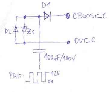
1) when input PWM is zero, "Energy Transfering" Capacitor is charged from OUT_C , and this energy/currrent is connected to Capacitor by Diode D2.
2) when input PWM is one=high=12V, Capacitor is shifted "up", and therefore Enenrgy is flowing (by Diode D1) to CBOOST_C pin.
Zener diode is NOT needed for normal operation, but is recommended for FAULT, switch-OFF... etc. conditions. This zener is protecting
CBOOST to not exceed +13V abs max. (This may teoretically happens when Transfer Capacitor will be charged AND if user switches OUT_C to GND or with FAULT/RESET to FLOATING position.)
Second part of schematic is voltage Levelshifter, transfering 3V logic to 12V logic. Simple solution is presented:
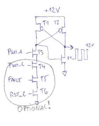
Schematic is simple, push-pull otput stage generates "hard"=low impedance output GND/12V voltage. For my application, to 100percent ON Time output stage C, I have used input signal PWM for channel A, because PWM_A is in this situation "switching" (I needed pulses to continuosly charge CBOOST_C). It is necesary to note, that transistors T4,T5,T6 are OPTIONAL, only theoreticaly super-mega-cerTIfied-ultra-safe design should use FAULT, RST_C PWM_C signals to form multiple input AND gate, BUT in practice, they are NOT needed at all IF!! Zener from schematic above will be powerfull enough, and if extra noise from switching and discharging of transfer capacitor is acceptable.
Unfortunatelly, to finish this design, it is necessary to choose correct size/value of Capacitor,and for this, it is "mandatory" forTI to answer Question, what is current consmption of each CBOOST pin of DRV8432 DRV8332 DRV8312 DRV8412 ..........
Thanks.


