This thread has been locked.

If you have a related question, please click the "Ask a related question" button in the top right corner. The newly created question will be automatically linked to this question.

Problem with DRV8301 and FAULT pin

Other Parts Discussed in Thread: DRV8301, DRV8312

I have a custo board with a DRV8301 driving a 3-phase PMSM motor. When I apply a fixed duty-cycle pwm to the three phases, everything works fine when phases A and C are >50% duty-cycle, and phase B is < 50%, and current drives through the 3 phases. When I swap the duty-cycles around, i.e. A and C <50% and B>50%, the FAULT pin starts to cycle on and off continuously with a 427us Hi time, followed by around 900us low, so a repetition frequency of 758Hz. The PWM frequency is 20KHz. The OCTW pin stays Hi during this state.

I've checked GVDD = 11 volts, DVDD= 3.3V, PVDD= 12V. There's a bit of noise on GVDD, but nothing very significant.

Any ideas on what could be happening ?

  • Hi Geoff,

    Have you tried reading the SPI status register to see if we can find some more details on what is going on? Also, would it be possible to get a scope shot of this happening, as well as a snap shot of your schematic/layout around the DRV8301.

  • Hi Nick,

    Thanks for your reply.

    I'm beginning to think that this is a layout problem, because I'm getting very inconsistent results.

    I've tried reading Status register 0, but I'm not having any success. I know my code to read the register is ok, because if I set a value in a different register and read it back with the code in the same position, it reads correctly, but only when the fault hasn't occurred. Once I set a breakpoint to hit this code when the FAULT line goes low, Status reg 0 always reads zero.

    Also, I'm now getting just a string of FAULT pulses as soon as EN_GATE is driven high (0.5ms hi/ 0.8ms lo) for about 10ms. I can try to send you a scope shot of this but what other signals and supplies should be monitored at the same time ?

    I think I must be doing something wrong with the layout, although I have definitely connected the DRV8301 pad to ground. I haven't found any documents that address the layout issue very thoroughly but it seems to be quite critical; I've so far not been able to get the buck regulator working at all.

    Can you give me some guidelines for things to check on layout ?

    Thanks,

    Geoff

  • Hi Geoff,

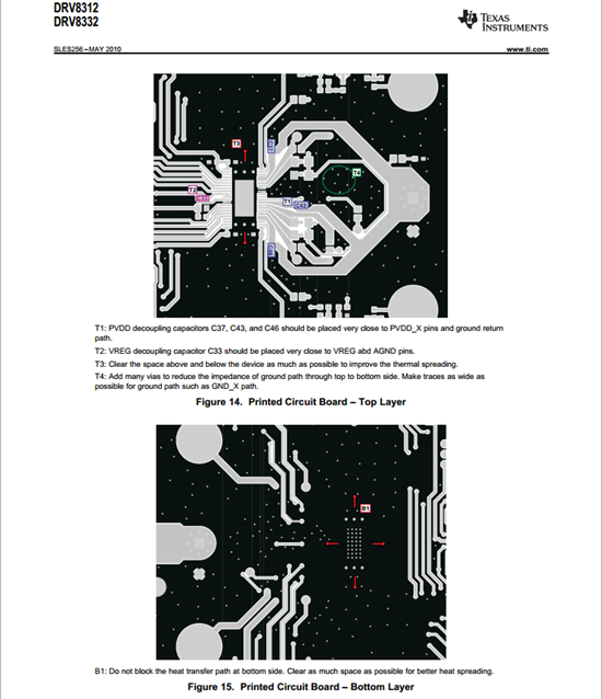
    The DRV8312 datasheet (pg. 22) has some good suggestions to follow. Be sure to check that all decoupling capacitors are placed as close as possible to the device and have a direct path back to the device GND (PPAD). The decoupling caps on the internal regulators must have a clean path back to AGND as well. This is an issue that we usually see in layouts. The buck regulator issue definitely points to some schematic/layout problems or a damaged chip. Has it ever worked?

    As snapshot of your layout may help to diagnose some of the issues.

  • Geoff,

    Here is some literature specific to the DRV8301 and layout considerations (http://www.ti.com/lit/an/slva552/slva552.pdf).

    Also,

    This thread discussed some similar issues.

    (http://e2e.ti.com/support/applications/motor_drivers/f/38/t/270459.aspx)

  • Thanks for both the suggestions Nick, I'll study it all and let you know whether I can see any obvious problems.

    I'll try doing a snapshot of the layout but I've hacked it around a bit fixing what I thought may be wrong with ground planes, obviously it didn't work !

    No, I've had two versions of my board now and on three different DRV8301's, I never managed to get the buck regulator working


    Geoff

  • Hi Nick,

    I've now studied the documents you suggested, and I also have a DRV8301-HC-EVM board which I've been looking at, along with its documentation, particularly the artwork of the board, and especially the ground planes.

    This is my understanding of the situation :-

    1.  The critical components for placement on the EVM board are C7,8,10,14 and 15. On this board C7,8 and 15 all connect to the top layer ground plane which goes underneath the DRV8301, and which the PowerPad solders on to. This top ground plane connects to a bottom layer ground plane via around 39 vias directly underneath the DRV8301. This top ground  plane has no connections back to the power ground terminal other than by the 39 vias throught to the bottom ground plane.

    2.  C10 and C14 don't connect directly to the top ground plane but via several vias each to the bottom ground plane under the DRV8301. I'm assuming that this equates to the 'star' connection recommended in document SLVA552 for all the capacitors C7 to C15.

    3.  The bottom ground plane under the DRV8301 connects via two paths forming a circular route back to the power GND connection and to C50, the large electrolytic across the power-in and ground terminals. One of these ground paths for the DRV8301 also includes the external current-sense op-amp components.

    4.  The motor return currents via the current-sense resistors, R80,81 and 82 have an almost separate ground path back to the GND terminal, altgough there is some mixing of the DRV8301 ground plane with this return path.

    5. The buck-regulator components use the same top layer ground plane connection as C7 to C15 back to the DRV8301 PowerPad.

    6.  The ground connections for the controller card and encoder signals connect to the DRV8301 ground plane on the top layer, but there is also a thin track connection back to the GND connection, close to the external sense amp components.

    Is my assessment correct, and as I haven't currently followed these rules in my layout, is this the most likely cause of my problems ? Have I missed out any critically important points because I don't want to lay out another board, only to find that it also doesn't work ?

    Geoff

  • Geoff,

    It looks like you have done a good job of understanding this issue. C5 and C6 are also critical components and should follow similar rules. C81, C82, C83 should be noted as well. Place these caps close to their assosciated high side FET.

    A more general summary of what you have found.

    1. PVDD decoupling caps (C5/C6/C7/C8) for the DRV8301 should have a direct return path to the device GND (PPAD) that is as short as possible. The longer the path the worse GND bounce/noise will affect the device (Vias add increased inductance/resistance so a path on the same layer is even more desireable).

    2. The internal reguator decoupling caps should have a direct return path to AGND and GND (PPAD). They are connected to the same net on the EVM but this is stated in the datasheet. This path is even more crucial as GND bounce/noise will have a larger effect on the internal logic.

    3. It is a good rule of thumb to stitch the TOP and BOTTOM GND planes together fairly heavily around the device (and board in general to reduce long return paths) in addition to the recommended PPAD vias. You can see this in the EVM layout. Use good sense here as you don't want to completely litter your board with vias.

    4. For the motor return current you want a clear direct path back to the Power Supply decoupling cap and input header. This can be a large current so a wide, short trace is highly recommended depending on your current requirements. Current will return through the sense resistors. This return path should try to avoid the DRV8301 and other devices (controllers) as the high power will also have high noise.

    These recommendations are all highly important and it looks like you have discovered them. (Remember C5 & C6 as well).

    The buck regulator not working is still worrisome. I would like to see you final schematic as I believe you might have an error with the configuration of the buck pins. Also feel free to post you final layout and we can look over it to try and spot any worrisome spots.


    Sidenote:

    Q: Why all this trouble?

    A. Unfortunately working with any motor is a highly noisy environment. We do our best to account for this in our drivers. But board layout/component placement is the single largest factor that can improve or degrade this. 


  • Hi Nick,

    Thanks for confirming that I've more or less got my assessment correct, and thanks for your general summary of the requirements.

    I'll definitely accept your offer of looking at my schematic and layout when I've re-done it, before I get my prototype board made. After all this trouble I don't think I can stand the idea of bulding another board and finding out it doesn't work !

    Regards,

    Geoff

  • Hi Eric,

    I've almost finished my layout of a prototype board following your recommendations and the general layout of the DRV8301 evaluation board now.

    Can you tell me what formats you can accept schematics and layouts in to give your opinion on what I've done ? My schematics are done in a fairly old version of Multisim, and I could send you the gerbers of the layout, if those are any use to you ?

    Regards,

    Geoff

  • Nick,

    Sorry I called you Eric, My excuse is that I was just doing an online chat with a guy called Eric !

    Geoff 

  • Hi Geoff,

    The easiest way for us is a pdf of your schematics and the gerber files.

  • Hi Nick,

    I'm attaching the schematic and gerber pdf's as suggested, and I'd be grateful if you could cast an expert eye over them before I commit to having another prototype made.

    Please let me know if any of the pdf's are no good, or if you need more information.

    Thanks

    Geoff5621.DRV8301 All Layers.zip

  • Geoff,

    A few comments,

    1. Could you just set the buck to 3.3V instead of using two different converters? Or do you need the 5V Rail?

    2. VREF should be set to the ADC ref from your microcontroller (just double checking)

    3. What is the purpose of R32 and R33 on PVDD1?

    4. Do you need the 10 ohm resistors on GH_X and GL_C? This may be a little high but depends on the FETs. The DRV8301 also has adjustable gate drive.

    5. A solid copper pour is best for the PPAD to GND connection.

    6. C22 should have a direct route back to the AGND pin. It is best to make this on the same layer.

    This is just what I can pick out.

    I have attached another helpful guide that is in the process of being put together.

    8168.DRV8301-2_Layout_Recs.pdf

  • Hi Nick,

    Thanks for the very quick reply.

    Here's my answers to your comments

    1.  I do need 5 volts as well as 3.3 volts to power a few things including a canbus chip and an external optical encoder.

    2. Although my VREF is labelled 2.5V, there is an option on this prototype board to select between 2.5 volts for external A to D's, and 3.3 volts for the micro's Vref.

    3.  It's missing off the schematic, but the junction of R32 and R33 goes off to an A to D input on the micro to measure supply volts.

    4.  The 10 ohm resistors are there to limit the rise time of the gate drive, which I thought was good to minimise noise on the board. I can remove them if you don't think it's a good idea.

    5. I'll get rid of the thermal reliefs on the PPAD.

    6. I'll alter the layout to connect C22 direct to AGND on the same layer.

    I'll study the layout document you sent the link to, thanks.

    Regards,

    Geoff

  • You may consider an LDO regulator off of the 5V rail for your 3.3V rail if the current requirements are low.

    The 10 ohms should be fine.

    Good luck!

  • One thing I forgot to ask earlier Nick, did you have a good look at the component layout around the devices associated with the buck regulator ?

    As I said before, I've already had two failed attempts at getting this going so I'd like to be sure there's nothing wrong with my current layout.

    Thanks,

    Geoff

  • I cannot see anything wrong in the Buck configuration but I might be missing it, possibly it was a soldering issue. I would just make sure to use solid fills when dealing with power traces, Ex. when you connect from the PH pins to PH trace.

    Another note, do you have pull up resistors for nFAULT and nOCTW?

  • OK, I'll make sure I have solid copper everywhere it's needed.

    Yes, I do have pull-ups on FAULT and OCTW, I had noticed that they're open drain outputs.

    Thanks