This thread has been locked.

If you have a related question, please click the "Ask a related question" button in the top right corner. The newly created question will be automatically linked to this question.

DRV8301 board layout

Other Parts Discussed in Thread: DRV8301

Good morning,

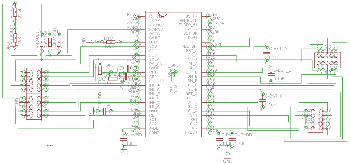
I am part of a team using the DRV8301 for a motor controller and we designed our own board layout. However, after reading some of the issues others had with their layouts, I am hoping to get some feedback on our design before sending it off to get manufactured. We mostly followed the example schematic from the DRV8301 datasheet.

Also, since we aren't using the buck, can we also remove PWRGD from the circuit?

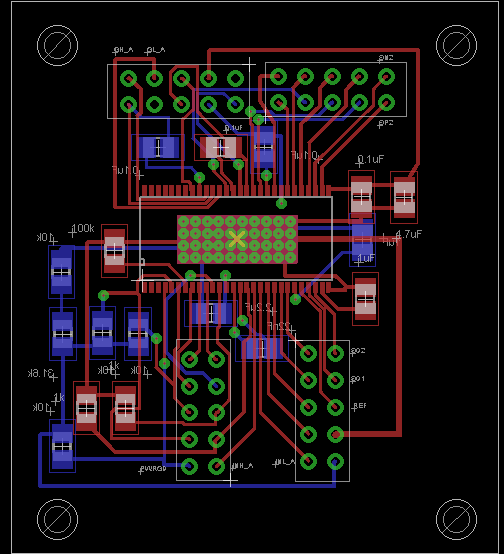
Thank you in advance,

Michael

  • Hi Michael,

    If you take a look at the end of the datasheet, there is a section on Layout Guidelines. Please take a look at this and the questions below.

    Right of the bat, it looks like you do not have a top or bottom ground plane. I would highly recommend these in motor design. Second, is this board driving FETs on another board? Long traces for the gate drive can cause issues due to parasitics. I would still recommend a pull up resistor on PWRGD. There is also a recommended land pattern for the thermal vias under the PowerPad in the datasheet.