Because of the holidays, TI E2E™ design support forum responses will be delayed from Dec. 25 through Jan. 2. Thank you for your patience.

This thread has been locked.

If you have a related question, please click the "Ask a related question" button in the top right corner. The newly created question will be automatically linked to this question.

DRV8301 Current Shunt Amplifiers - Output Noise

Other Parts Discussed in Thread: DRV8301, BOOSTXL-DRV8301, DRV8301-69M-KIT

Hi,

I'm using the current sense amplifiers to measure the bridge current on my PMSM FOC motor application, but when I look at the values from the ADC, they're noisy, even with just fixed duty-cycle values into the bridge.

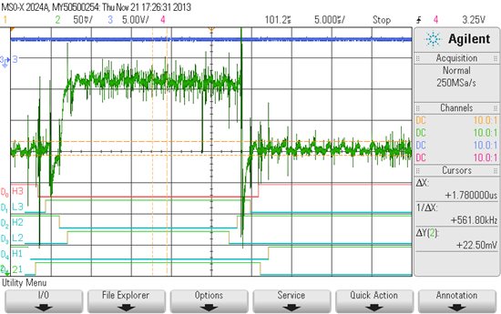
I'mm attaching a scope image of the output of one of the sense amps, and you'll see that there's a 22mV ripple on the trace, with a ripple frequency of around 560KHz.. I believe that's the switching frequency of the buck converter, so presumably it's related to that.

I think I've been careful to follow your layout guidelines and component values, and I certainly have the AVDD capacitor very close to the pin and ground plane.

Any suggestions as to what I might be doing wrong ?

Thanks,

Geoff

  • Hi Geoff,

    Do you mean values from the Amplifier? Where are you measuring this on yor board? Where is the ground probe located?

    Can you show a picture of your layout with these two points highlighted and possibly the schematic?

  • 0458.DRV8301.pdfHi Nick,

    Sorry I wasn't very clear. What I meant was that the traces shown on the scope plot are going into ADC channels on the micro, and when I log the output values from the ADC, they are noisy. The DRV8301 is beinh driven with fixed PDC values to eliminate any affects from the current control loop outputs, and the sample time of the ADC's is locked to a fixed point in the pwm duty-cycle.

    I'm attaching a photo of the board (and relevant part of my schematic), showing the scope probe and ground connected for the measurement. The ground, just in case it's not clear on the photo, is connected to the top ground plane which extends under the 8301, then out at the top and on to the buck converter components.

    You helped me a while ago when I was having trouble with the 8301 ground connections, so I have tried to follow your recommendations on grounds and component placement.

    Hope this additional info is of use,

    Regards,

    Geoff

  • Hi Geoff,

    Some more scope captures may help determine the source of the noise.

    Some things to look at.

    1. Scope capture of buck output before and after inductor with amplifier ouputs

    2. Scope capture of high side of sensor resisotor or wherever the inputs to the amplifiers are with the amplfier outputs

    3. Scope capture of amplifiers supply/reference voltage with amplifier outputs

  • Hi Nick,

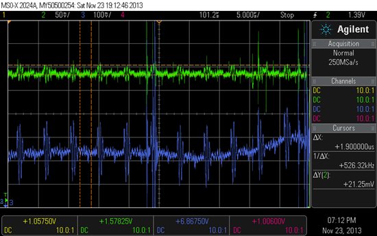
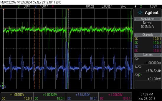
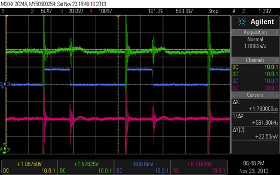
    I've captured the points you suggested and pics are attached.

    Current sense amp output is always channel 2.

    "amp_avdd" shows amp o/p and AVDD pin.

    "amp_ref1" shows amp and REF pin, which is connected to the 3.3 volt supply

    "amp_sense_res" shows amp and high end (SP1) of sense resistor

    "amp_buck" shows amp and PH outputs on chan. 3, and buck 5 volt o/p at o/p caps.

  • Geoff,

    I am not seeing any images attached.

  • Sorry, I'll try again.

    These are in the order amp_avdd, amp_ref1, amp_sense_res, amp_buck.

    Hope they've come through this time

  • Hi Geoff, it looks like there is a fair amount of noise on the sense resitor as well. This may be propagating through the CSA. Are these shots with a motor connected?

  • Hi Nick,

    Yes, it's with a motor connected, although there was a 50:50 duty cycle on all 3 phases, so the motor current was very low.

    The only observation I made was that the sense resistor noise seems to be a higher frequency and unrelated to the buck frequency, whereas the other plots show noise in sync with the buck..

    Geoff

  • Hi Nick,

    I've tried lashing-up a BOOSTXL-DRV8301 board to the rest of my circuitry, bypassing the DRV8301 that's already on the board. The noise on the amp outputs has reduced very significantly and the buck frequency ripple has gone.

    From this, I guess we can assume that I've got something wrong either with component values or the layout, although I did think that I'd been pretty careful with both of these. The only other difference is that the buck regulator on the BOOSTXL is more lightly loaded because it's not powering the rest of my circuit, so I guess I could take the 3.3 volts off the BOOST-XL to power my circuit to test this.

    Is there a schematic, BOM and layout available for the BOOST-XL, so that I can make sure that my design is 100% correct ?

  • Thanks for the information Geoff.

    The hardware design files can all be found in the tool folder for the BOOSTXL-DRV8301. There is a hardware files zip folder near the bottom of the page.

    Do you mind posting your schematic and layout again? I wil give them another look over.

  • Hi Nick,

    I'm attaching the schematic and layout as requested. One question I have is how critical are the component values around the buck regulator; I was thinking particularly of the LC filter values and types ?

    Incidentally, I've bought the DRV8301-69M-KIT now. It seems pretty clear that with your INSTA-SPIN and SPIN TAC routines, this will be the best long-term solution, even though it means learning about CCS and TMS processors.

    Regardless of the processor, I obviously still need to get the DRV8301 part of the circuit working correctly.

    Geoff8484.DRV8301Layout.pdf5516.DRV8301schematic.pdf

  • Hi Geoff,

    I don't see any issues that stick out immedietly in your schematic. I don't think LC filter values should be to large of a concern. I would be more concerned with layout (perhaps coupling from another line). Since the BoosterPack has no issues this would definitely point to a layout or manaufacturing issue.

    Do you mind sending the gerbers. I cannot tell much from that PCB image. You can send to me in a private message if desired.

  • Hi Nick,

    I'd be happy to send you the gerber files, in a private message if that's ok with you, so how do I do that ?

  • I believe I must be a friend to you on E2E. I just send you a request. Accept that and you should be able to start a "conversation" aka send a message on E2E.

  • Nick,

    Don't know whether it worked but I tried sending you the gerber files as requested

  • Geoff,

    The end of the document has some useful tips on selecting components for a switching buck regulator. I am sure there are also other resouces out there.

    http://www.ti.com/lit/ug/slvu257a/slvu257a.pdf