hello,
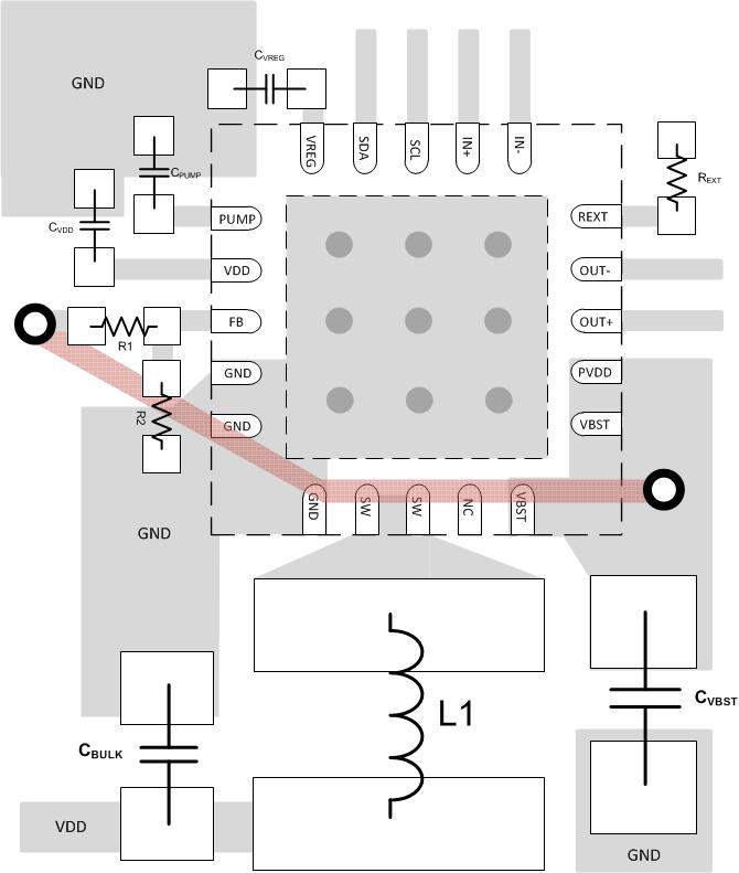
What makes it necessary to put the feedback resistors near the FB pin on the DRV8662? I burned out several chips until I changed my design to take this into account.
1) I built a PCB design putting the feedback resistors near the Vboost pins, with a longer lead going across the chip and to the FB pin. This circuit failed spectacularly! Before I put a current limit on my power supply, the first couple of chips shorted out and were damaged (it appeared that the diode in the SW circuit burned out). Once I put a current limit on and looked at what was happening under a scope, it appears that the boost converter oscillator never started - the SW pin went to ground and never released.
2) I then copied the PCB design from the evaluation board, moving the feedback resistors next to the FB pin. Circuit works beautifully!
This cost me several days of debugging. I'd like to understand why the circuit is so sensitive to the position of the feedback resistors, if just to make sure that my design is well within spec?
Also, what is the reason for the 105V limit - is there an internal component that will fail beyond that voltage?
best,
Fred