This thread has been locked.

If you have a related question, please click the "Ask a related question" button in the top right corner. The newly created question will be automatically linked to this question.

DRV8301 ignores low-side FET input signal

Other Parts Discussed in Thread: DRV8301

Hi,

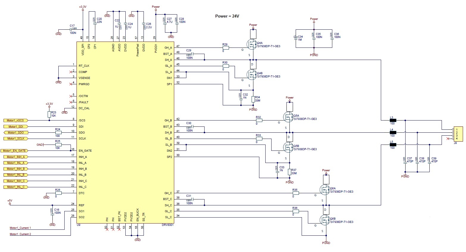
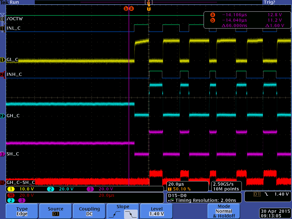
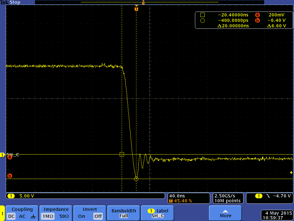
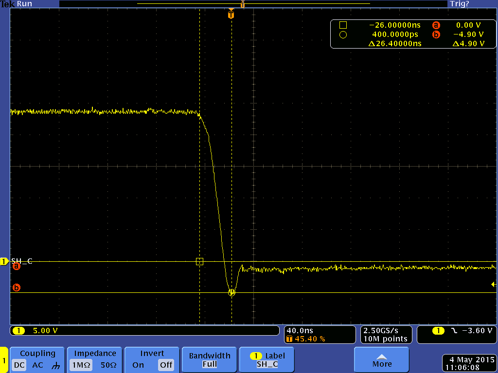
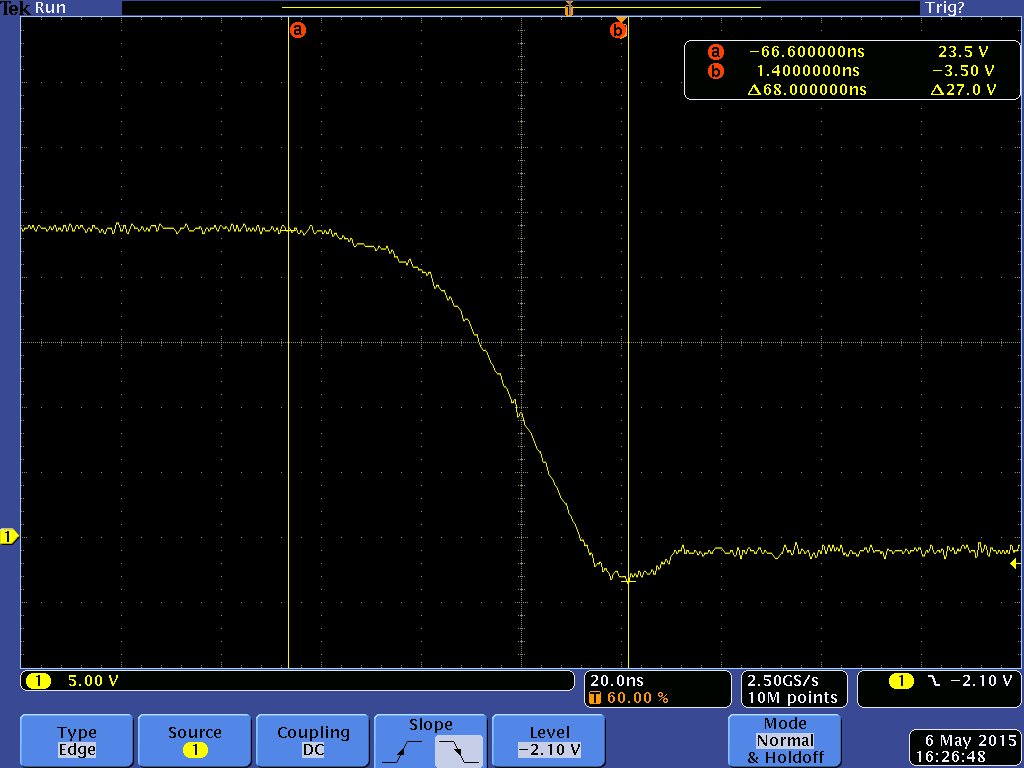
I’m using the DRV8301 to drive a three-phase BLDC motor in “6-step trapezodial commutation”. Due to the trapezoidal commutation, one of the three phases is (in relation to the hall-sensors) inactive (low/high-side FETs disabled). With this situation, the DRV8301 seems to have a problem. When the motor starts turning (change TargetPosition of the position control-loop in uC), and the hall-sensor changes his state, the inactive phase needs to be activated. To ensure loading of the bootstrap capacitor, I switch ON always first the low-side FET. And here is the problem. Sometimes the DRV8301 ignores the low-side gate signal --> the LS gate output doesn’t do anything! In consequence of this, the bootstrap capacitor doesn’t charge and the first time the high-side FET switches, an OC failure occurs.

Is this a known issue of the DRV8301?

I searched the support forum and found an interesting post “DRV8301 : Trickle Charge Circuitry and Internal Handshake”. It seems he had exactly the same problem. I wonder if there was a solution on this problem.

regards,
Marco

  • Hi Marco,

    These problems do appear very similar. Let me investigate into the post you linked and see if I can find any more information.

    In the meantime, I have a few questions. 

    • What supply voltage are you operating at?
    • Can you provide an scope capture of the Hi-Z phase when it transistions? I would like to see what voltage it is at before the low-side tries to turn ON.
    • Can you provide a snapshot of the schematic around the DRV8301? We can set up a private communication over E2E if it is confidential.

  • Hi Nick

    Supply Voltage is 24V. Attached you find the schematic of the DRV8301. I have to take some scope captures. I will send them later.


    Marco

  • Hi Nick,

    I've done some measurements. Attached there are two screen captures of the scope. The first one shows normal operation. The second one shows the moment, when the DRV8301 ignores the low-side input signal. Measurements were done referenced to GND. So I added a math-calculation to get the real high-side signal on the FET.


    Normal operation:


    DRV8301 ignores low-side input signal:


    regards,
    Marco

  • I made an additional test with disabled over-current protection. The behaviour stays the same. Low-side input signals are ignored.

  • Hi Marco,

    This is quite unusual. I cannot detect any difference between the two scenarios. We have seen an condition somewhat similar to this (low-side not enabling) but it was related to power sequencing of the device. It did not affect normal operation after the device was successfully enabled and we have no seen this anywhere else.

    Can you try an experiment for me? Can you add a 1MOhm pull up resistor to PVDD1 from each BST_X pin and see if the issue still occurs? You can solder from the BST_X side of the bootstrap capacitor to PVDD1.

  • Hi Nick,

    Since I don't have the chance to change the hardware short-term, I am looking for a bugfix in FW.
    I reduced yesterday the gate drive peak current to 0.7A. Since then I cannot reproduce the failure any more. Is it a possibility that the DRV8301 is internally disturbed by the higher gate currents? As a gate-resistor I have zero-ohm chip resistor, to have the possiblity to change in future. On the evaluation board of the DRV8301 seems to be 1 ohm gate resistors.
    I also checked the layout. I use a 4-layer layout with proper ground an power-planes. In the picture you see the placing. During the tests the second DRV8301 was disabled, so there is no interference between the to channels.

    Have you ever seen chip internal disturbance by gate signals.


  • Marco,

    Can you take a scope capture of the MOSFET Vds slew rates with the higher and lower current settings? What is the MOSFET PN you are using?

    The default setting (1.7A) is generally fairly high for a standard MOSFET. This can lead to very fast slew rates which introduce switch node ringing and other issues. We will generally lower the setting and introduce series resistance to reduce the strength of the gate drive. 

  • Nick,

    PN of the MOSFET is SI7938DP-T1-GE3.
    I measured Vds of the low-side FET of phase C (Designator Q6B) with 1.7A and 0.7A gate-current setting. As you can see, there is ringing and there is a difference between the 2 settings. Altough the difference is not that distinct.

    Q6B_Vds_switchOFF_1.7A Setting

    Q6B_Vds_switchON_1.7A Setting

    Q6B_Vds_switchOFF_0.7A Setting

    Q6B_Vds_switchON_0.7A Setting


    Do you think I should reduce the ringing with the gate resistor?

  • Hi Marco,

    Yes, I would increase the gate resistance and reduce the gate drive strength. The ringing that you are seeing is still fairly severe.

    I would target a slew rate of ~100ns to try and reduce the ringing furthur.

    Can you try the 0.25A setting with 10Ohm of series resistance?

  • Hi Nick

    I tried different combinations of gate resistor and current settings. 0.7A setting and 10Ohm of series resistance seems to be a good trade-off between overshoot on Vds and fast switching. See attached the measurements of Vds. What do you think?

    switch-OFF

    switch-ON


  • Hi Marco,

    These slew rates seem reasonable.