This thread has been locked.

If you have a related question, please click the "Ask a related question" button in the top right corner. The newly created question will be automatically linked to this question.

DRV8301 charge pump problem?

Other Parts Discussed in Thread: DRV8301, BOOSTXL-DRV8301

hi, I am doing a BLDC motor driver design using DRV8301, and my circuit is similar to Boostxl-drv8301 kit except the FET used. Here is schematic and PCB file:

Cadstar-drv8301.pdf

https://e2e.ti.com/cfs-file/__key/communityserver-discussions-components-files/38/stpmtc001v03_2D00_gerber_2D00_150910.7z

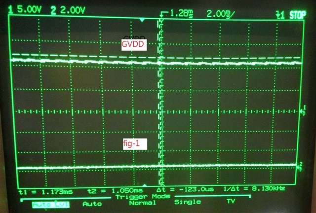
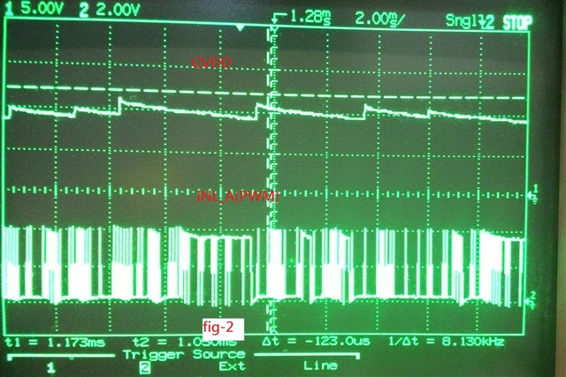
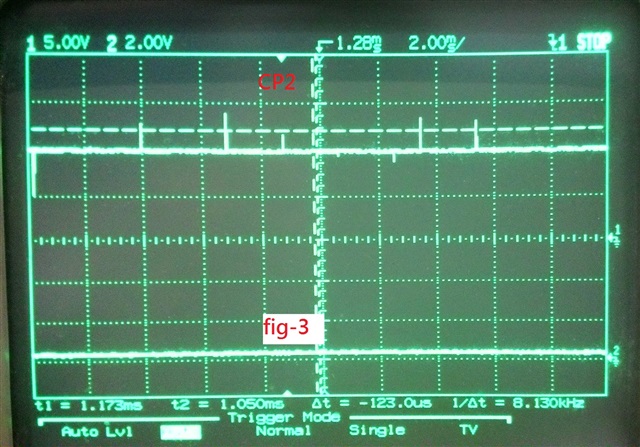
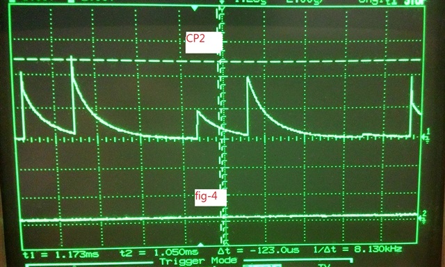
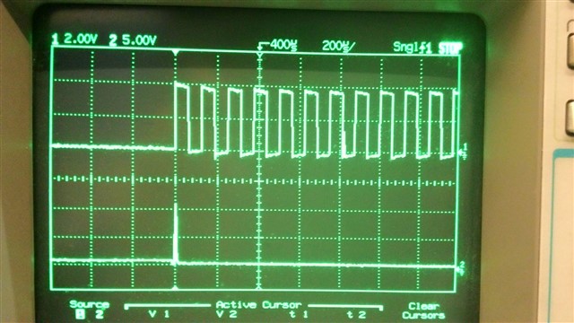
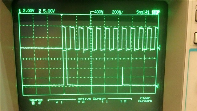
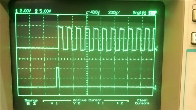
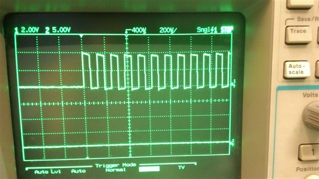
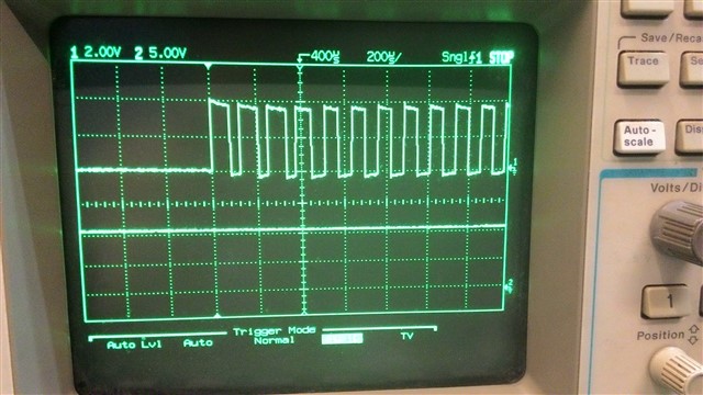
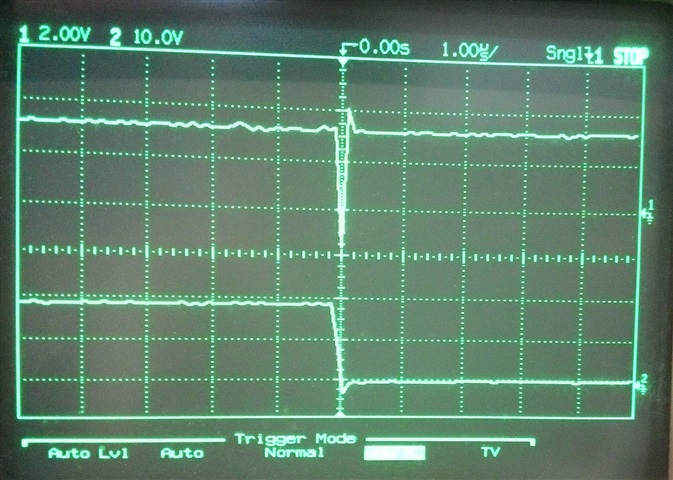
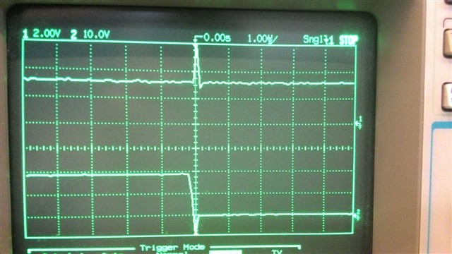
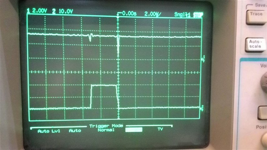
But when I use TMS320f287 to control it, the gate driver signals did work properly. And I have compared to the proper worked kit, I think it's caused by charge pump problems. The charge pump and the GVDD wave form is below:

The above wave form are taken from the Drv8301 GVDD, CP2, INL_A(PWM) pins. Before the PWM signal enables, the VGDD is about 8V, and CP2 is biased at GVDD with some pulse as in fig-1, fig-3. And when PWN is enabled, the GVDD has a lot noise as in fig-2, and the CP2 can not be biased at GVDD as I compared to the working Boostxl-drv8301 demo kit.

I thoght it was caused by the PWM frequency and high Qg of FETs, I have lower down the PWM frequency to 8Khz and use the low Qg EKI06108(Gg 36nC, ). 

But the gate driver signals still is not working. We have made several boards, some boards can work good but for just a few seconds then the waveform is bad again.  Is there any suggestions? 

  • Frank,

    How are you connecting the PowerPAD of the DRV8301 to the PCB? It is critical that this make a good electrical connection to PCB GND as this is the device main GND pin. I don't see a pin for it in the schematic.

  • Hi, the GND pad is connected as hidden power pin of the symbol. And in PCB I place a piece of copper and many vias under the DRV8301. I have de-soldered one DRV8301, and I am sure that the solder paste under DRV8301 is pasted.
  • I have tried the enlarge the Cap at CP2 from 0.022u to 2.2u, the voltage on CP2 is increase to be bias at 5V but still not as high as those working one. The working Drv8301 the CP2 is bias at about GVDD level. The bypass at GVDD is enlarge also, the ripple on GVDD is improved but the gate driving signals are still not working. I have set break point is software the any error flags set in Status1 will be stopped, but the Status1 does not report any error!
  • Hi Frank,

    Ok, thank you for checking.

    Let's try and rule a few things out as we try and find the root cause.

    What is the input supply voltage? How is it being supplied?

    With PVDD1 power supplied and EN_GATE = HIGH can you measure the DVDD, AVDD, and GVDD pins and report back their voltages?

    You said the GVDD is 8V before the input is supplied, this is quite strange. It should be around 11 V.

  • PVDD1=12V, supplied with power supply. => DVDD is 3.3V, AVDD is 7V, GVDD is 10V. GVDD 8V was not measured with accuracy, for smaller voltage scale it's about 10V.
  • Thanks Frank,

    These values all seem nominal. Can you now try and toggle one of the phases with no load connected and capture the waveforms (SH_A, GH_A, GL_A, GVDD).

    Trigger on the first rise and falling edge of the phase. We want to see the first transistions.

  • PWM_AH vs SH_A:

    pwm_ah vs gah,gal:

    pwm_al vs gal:

    pwm_al vs gvdd:

    It seems the only the first rising edges are good

  • I have added two 220U/63V cap to PVDD1, still no help. It seems like the output being shut down, but the SPI does not report any OC error. I have set the OC mode to be report only but it's the same. The Gate current is also increased to 1.7A by SPI set up. Does the FET Qg maters? I have compared the FET used in Bootxl-drv8301 , the Qg is about 20~30 nC, the Qg of the FET I am using is about 30~40nC, will it be so critical?

  • Here are two more wave form from ENGATE, GAH:

    The spike on ENGATE is so high that the TMS320F287 will lost control by ICE when PWM out out is enabled by setting run at GUI Composer. The spike does not come from coupled parallel signal. I have tried the cut out the trace of ENGATE from TMS320F287 and connected it direct to 3.3V, but no good. Add a 33u cap to ENGATE will help, the GAH output wave form's good working period is prolonged but still not completely OK. 

    After I cut trace from TMS320f287 and jump a wire to 3.3V, the pin on ENGATE still has spikes:

    What might cause it to behave so? Is the improper DRV8301 layout will cause such big spike? 

  • I have tried to lower down the input voltage from 12V to 8V, the proper working duty will increase. It seems DRV8301 is mall-functioned due to the high voltage gate switching, is there any means to fix it other then re layout? 

  • Moving from 20-30 nC to 30-40 nC should not be an issue. Layout will have a significant effect on the performance of a switching power design. Can you try reducing the gate drive current? This will reduce the slew rate of the MOSFETs.

    Can you verify that none of the external MOSFETs are damaged or a short? Oftentimes when only a short spike is seen this points to an OC event.

    If the DRV8301 has been damaged by a high voltage transient it will need to be replaced.

  • 1.There are serial resistors  at each gate drive signal, I see some TI schematic place a one ohm on it, currently I am using zero, what value would you suggest me to try?

    2.The SPI interface is OK, will the DRV8301 be damaged at driving parts only but SPI part still OK? 

  • 1. I would recommend adjusting the SPI setting to 250mA and using a 10 Ohm resistor initially to limit the slew rate.

    2. It is possible for the SPI to be working and the gate driver to be damaged. It will be difficult to tell if there are still issues in the application. I would recommend adjusting the slew rate and verifying on several boards.