This thread has been locked.

If you have a related question, please click the "Ask a related question" button in the top right corner. The newly created question will be automatically linked to this question.

DRV8305-Q1 faults

Other Parts Discussed in Thread: DRV8305

I'm observing fault conditions I don't understand.

On powerup, after chip is configured, I will see a 'warning' condition (fault line toggles), which is cleared by reading register 1, the status register.  The status code is 0x10, which indicates 'charge pump undervoltage'.

By reading register 1 I clear the warning (/FLT is high).

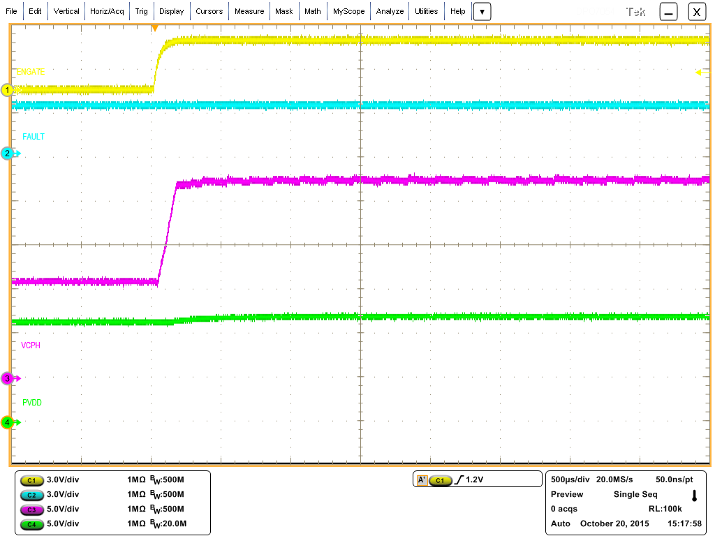
As I continue my startup code, I eventually run the code that enables the chip.  As soon as I enable the chip, I get into another 'warning' condition (fault line toggles).

This time, however, when I read the status register I read 0, indicating no warnings/faults, AND the 'warning' does NOT clear.

So, it acts like I have a warning that the status register does not report.   ???

I have set up register 9 with WD_EN = 0.

This seems to have something to do with enabling the chip.  Why does that matter?


  • Chuck,

    Let me look into this Monday morning and I will report back.

  • Here's some more info.

    I'm using an emulator on my board for debugging.  We're using a one-shot triggered by a software loop to control the 'EN_GATE' of the 8305; this allows us a quick way to disable the chip.

    If I set a breakpoint with my emulator, it will stop the retrigger on the one-shot, so the enable signal to the 8305 will time out.

    When I look with a scope I will see that I have a fault condition.  But, is this fault condition 'real', or is it because I an no longer enabling the chip?

    That is, does disabling the chip cause a fault condition?  When I am able to read a non-zero status back from the chip, it always seems to be 0x10,

    indicating a charge pump undervoltage condtion.  All power supply voltages are present and stable.  PVDD is 12 V.

    Also, we have a pre-production chip -- part number starts with a P, if that matters.

  • Nit picking. On p. 4 of the October revision of the datasheet, VCPH, pin 38, calls for a 0.47 uF cap. On p. 5, VCPH calls for a 2.2 uF cap. We're currently using 2.2 uF. Once the chip is up, does this matter?
  • Thanks for the typo catch. It should be 2.2 uF. The VCPH cap is used to supply charge for the switching high-side gates. The charge pump replenishes this cap. It will mainly determine how much ripple shows up on the regulated VCPH supply.

  • Chuck,

    Just to get some more details. 

    When do you first see the charge pump undervoltage warning? Is this immediately after power up or after you configure the registers? Is EN_GATE low during this process? The charge pump should not even be enabled until EN_GATE is taken high. What voltage is your supply and what is the ramp rate?

  • I first see the warning the first time I enable the chip.  All chip configuration is done by then.  From our end, I write to a 1-shot from a software loop to keep the chip enabled.  I never see enable go low, once I start writing to the 1-shot.

    I find that I'm getting continual charge pump undervoltage warnings.

  • Chuck,

    What is the PVDD power supply voltage?

    What is the value of the flying caps (CP1, CP2)?

    How long do you wait after EN_GATE low->high before you begin switching the gates?

    Is there any external load on the VCPH charge pump?

    One theory is that the VCPH ramp rate is to slow and the DRV8305 charge pump monitor is activated before it reaches the final regulation voltage. The CP monitor has an ~1ms delay after EN_GATE before it begins reporting the status of the charge pump. This is typically sufficient time to allow the charge pump to ramp up to PVDD + 10 V assuming no load is present.

  • PVDD=12 V.

    CP1=CP2=0.047 uF.

    We are not switching the gates.  We begin switching when we 'enable' OUR drive (this product), and the fault/warning is occurring without even attempting to 'enable' our drive.

    No external load on VCPH.  There would be a load only in the event of fault conditions; power supply overvoltage or reverse voltage.

  • Chuck,

    Can you get a scope capture of the EN_GATE pin and VCPH pin when you enabled the DRV8305 (can trigger on EN_GATE rising). Preferably at ~500us timescale.

  • Not easy to get a scope capture.  But, here's what I see.

    On enabling the chip, I see VCPH go from ~12 V. to ~22 V., in a ramp of ~240 usec.

  • Here's my latest theory.

    When the chip is enabled, the charge pump gets powered-up and takes ~240 us. to ramp up.

    I believe that charge pump UV warnings are being generated until the charge pump has ramped up.

    Is that true?  I believe I'm detecting that with breakpoints/debugging code, using my emulator.

    I think what I need to do to fix it is to read the status register, to clear the warning, until I don't see any more warnings.

    The problem I have is that this SPI channel is shared; so I can't continue to read the status register.

    At some point I give up the SPI channel, and it's reconfigured for runtime use by a different chip.

    Here's another issue.  Apparently the status register gets updated only every ~60 us. or so, so I can't continually read the status register to

    see if the warning has expired; I have to read it, wait, read it, wait, etc.

    Does this sound like a likely explanation/solution?

  • Chuck,

    The 240 us sounds typical. The charge pump should not be generating UV warnings though, this is unexpected.

    Even if it did generate a warning on the power up. The first read of the registers after powerup should clear the warning and it would not reassert. It should only reassert if a real charge pump UV condition is present.

    Below is a waveform taken on our EVM board showing a normal gate drive power up sequence EN_GATe LOW to HIGH. You can see VCPH rising and FAULT does not ever assert. I do not see any warnings either.

    Can you try and get a similar waveform with EN_GATE, FAULT, VCPH, and PVDD. Have you tested this behavior on multiple PCBs? Is it similar on them all. 

  • I've changed my scheme. Now I enable the chip, then configure the chip, then read the status register to clear warnings. Now we're working OK. I found that I had to have some software delays, after I enabled the chip, before I cleared the warnings. If I did not have this delay, and tried to clear the warnings immediately after enabling the chip, I would have warnings on the /FLT line.
    To me, this meant that you had to allow for some time for the warnings to assert themselves. When I enable the chip and then configure the chip, the software delays associated with the configuration appear to be sufficient such that reading the status register clears the warnings.
    If I don't allow this software delay, and read the status register immediately, I will see a toggling fault line.
    The description for the fault warnings indicates that there is a 60 us. cycle, which seems to say that faults won't show up immediately. I don't know if this is true for both the fault line and for the status register, but I found I had to introduce delays, after enable, to be able to clear warnings.
    This scheme works for us.
  • Chuck,

    Thanks for the update. We will see if we can make the datasheet more clear in this regard.

    The 56 us pin reporting pulse is for the warning pulse from the driver. When the DRV8305 signals a warning on the FAULT pin it uses a square pulse with a period of 56 us. When a fault is being reported the FAULT pin is held low.