This thread has been locked.

If you have a related question, please click the "Ask a related question" button in the top right corner. The newly created question will be automatically linked to this question.

DRV8432 TEC Drive (parallel full bridge mode)

Other Parts Discussed in Thread: DRV8412

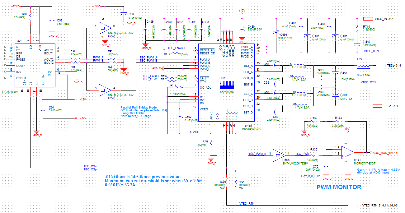
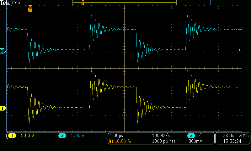
We are having unexpected behavior from this device and would like some help figuring out why.  Essentially we have complimentary PWM inputs driving the device and yet we fail to seen any significant current.  Both sides of the bridge appear to be turning on/off together.  There is also significant ringing on the outputs.  There is no evidence of overtemp or overcurrent faults.   

Unfortunatley although I have waveforms and a schematic I am unable to paste these into this forum due to security restrictions in the company webserver.  If you could provide an email address I would be happy to send or possibly upload to another location. 


  • Hi Jack,

    We will contact you with instructions on how to send them shortly.
  • Adding files to post.

  • Additional information:

    We are continuing to debug this circuit and found that shorting the 68uH inductor (L59) at least results in the 8432 behaving better, i.e. it is passing current. L59 is a remnant from an earlier DRV8412 implementation that was inserted to smooth the ripple on the current.

    I don’t have updated waveforms however the ringing on the outputs remains significant and I think is impacting the current sensing at the PWM chip because the control loop doesn’t appear to function except at very low current levels.

    I am aware of a few things that we have yet to try and that is increasing the Bulk capacitance as well as installing the DNI capacitors on the output. There is also a problem in the layout where the connection between the ground pins and the sense resistors (on the back of the board) is unfortunately a standard 12mil via. This is not easily reworked and I don’t know if it could be contributing to the problem, it can’t help.

    The value of the sense resistors is also greater than the recommended sub 10 mOhm and I am also considering making changes here.

    If you could provide some insight regarding best opportunity for minimizing the ringing, that would be a good place to start. Obviously if you see anything egregiously wrong with the circuit, please let me know. I can send gerbers or a Pads database if you like as well.
  • Hi Jack,

    There may be another problem with the control loop. Please note section 7.4 of the current datasheet.

    In operation modes 1, 2, and 4 (CBC current limit is used), once the CBC current limit is hit, the driver will be deactivated until the next PWM cycle starts. However, in order for the output to be recovered, the PWM input corresponding to that driver in CBC must be toggled. Because of this, CBC mode does not support operation when one half-bridge PWM input is tied to dc logic level.

    Is it possible that the current limit is reached, and U22 is getting stuck? This would prevent the outputs from being re-enabled.

    With respect to the ringing, please refer to the post ( LINK ). In the post there is a link to an application report on how to reduce ringing of NexFET MOSFETs. Perhaps some of the techniques can be applied to your system.

  • Hi Rick,

    We have resolved the problem.  Part of it was in the control loop as you suggested and was fixed in software; once that was resolved, the ringing was almost completely eliminated by populating the 4 capacitors at the output with 10uF devices.  There was some interesting interaction between the inductors that led us astray.  The final implementation continues to use the output inductor as it provides the current smoothing we were seeking.  Thanks for your assistance.