This thread has been locked.

If you have a related question, please click the "Ask a related question" button in the top right corner. The newly created question will be automatically linked to this question.

DRV8305 VDS monitor fault (how to reduce VDS)

Other Parts Discussed in Thread: DRV8305

Dear all,

I use DRV8305 to control brush-less motor.
When the motor speed is controlled to be down drastically in order motor to be stopped, VDS monitor fault occurs.
Motor speed is 1200rpm before I start motor speed down.
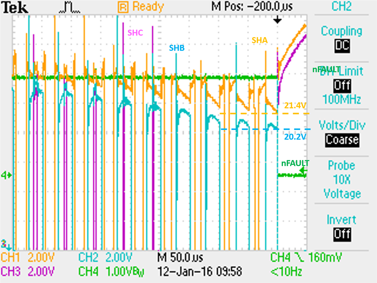
VDS monitor fault for high side FET (A, B or C) occurs with the following waveform.
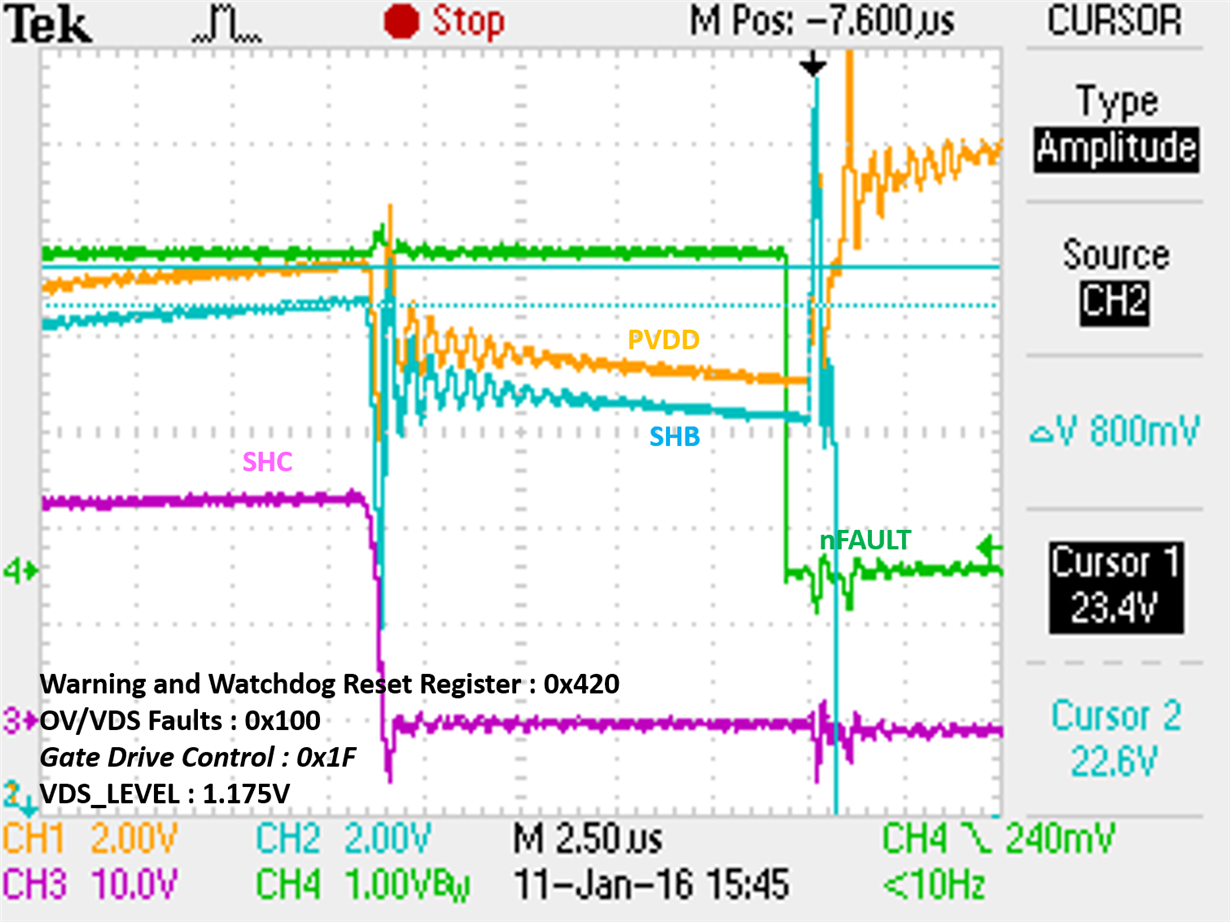
According to the above waveform, PVDD drops and so two 470uF capacitors are added (total four 470uF capacitors are used now.)
In the result, rate of VDS monitor fault is decreased but VDS monitor fault for only high side FET B sometimes occurs with the following waveform.
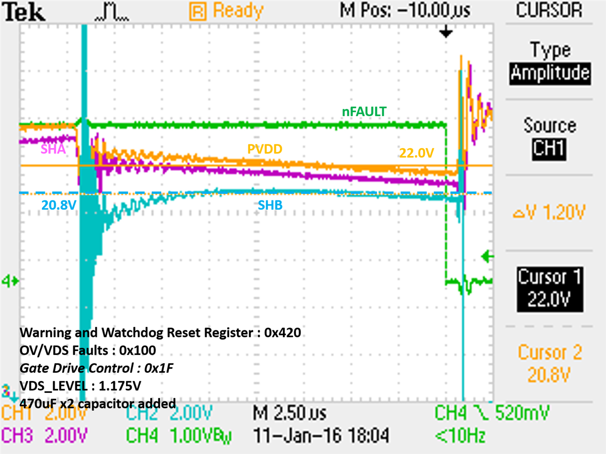
(My question)
1. Do you have any idea why FET B VDS is so high and VFS monitor fault for high side FET B occurs?

2. Could you tell me how to reduce VDS? (For example, adjusting slew rate prameters?)
I think VDS_LEVEL 1.175V is still so high for my FET because the FET Ron is small(1.4mOhm) but VDS monitor fault occurs.

Here is the setting and my PCB information.
[Control registers setting]
HS Gate Driver Control: 0x366
LS Gate Driver Control: 0x377
Gate Drive Control: 0x1F
Shunt Amplifier Control: 0x1A
and other registers are default.

[external components]
external FET Ron: 1.4mOhm
shunt resistors : 2mOhm

  • Hi Shirai-san,

    Does the VDS fault occur only on high side FET B? If so, could there be something in the layout affecting this FET?

    Have you compared the VDS of high side FET A and C to FET B? Are they consistent?

    Is it possible the gate to drain voltage is less on this FET?

    Are you comparing PVDD to FET drain using the device VDRAIN pin and the drain of the FET? If not, would you please capture the signals directly at the pins and provide updated scope captures?
  • >Does the VDS fault occur only on high side FET B?

    Yes. Other VDS fault dosen't occur.
    >If so, could there be something in the layout affecting this FET?
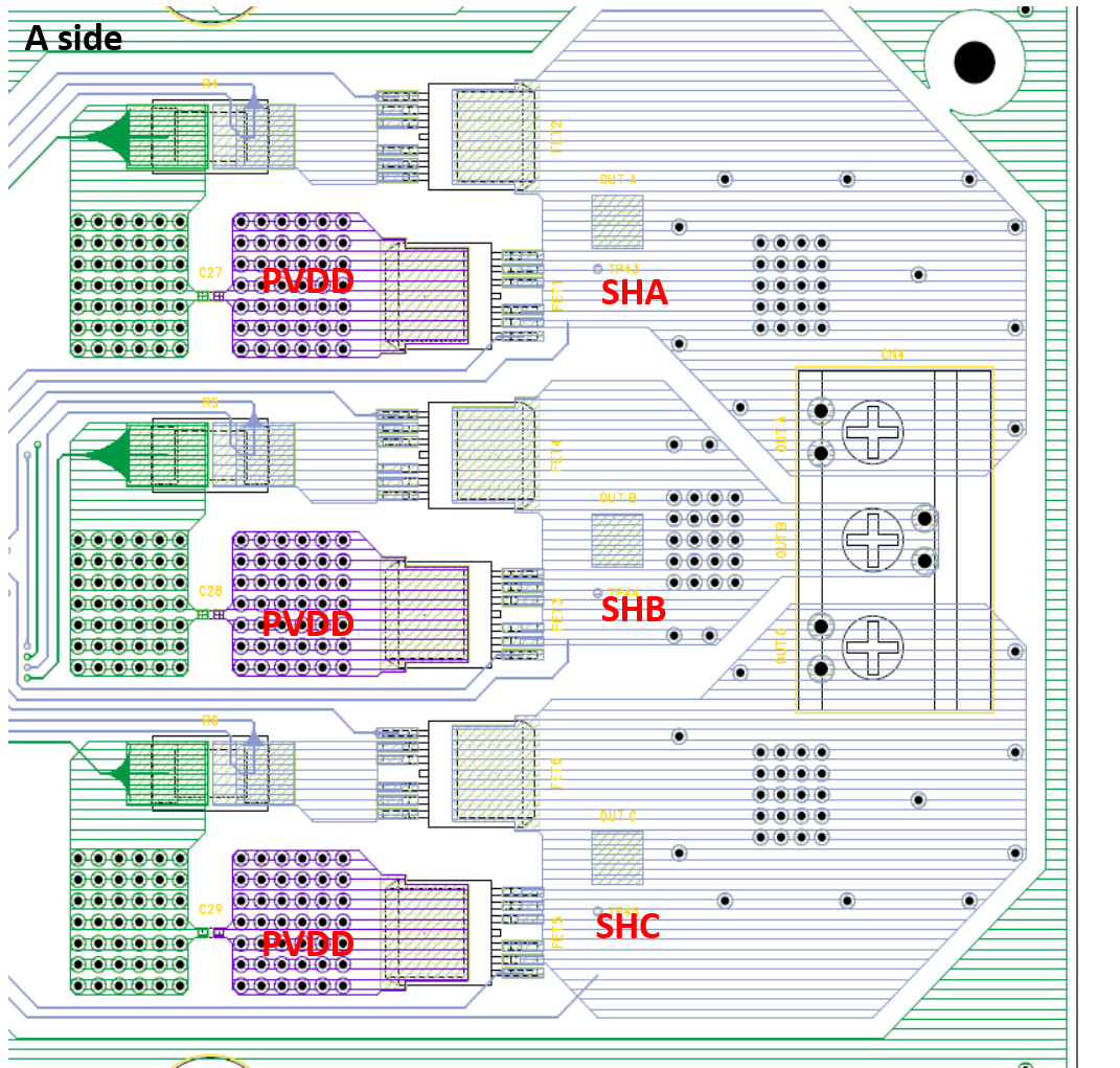
    I don't think the layout affects FET B. Here is the layout near FET A, B and C in out PCB. Could you check the layout and give me advise if you have something to tell me.

    >Have you compared the VDS of high side FET A and C to FET B? Are they consistent?
    When VDS fault occurrs, SHB always looks less voltage than SHA and SHC.
    The following waveform was captured when VDS fault on high side FETB occurs.

    I'll capture the gate to drain voltage, PVDD to FET, VDRAIN later and post them.

    Best regards,
    Shirai

  • >Are you comparing PVDD to FET drain using the device VDRAIN pin and the drain of the FET? If not, would you please capture the signals directly at the pins and provide updated scope captures?
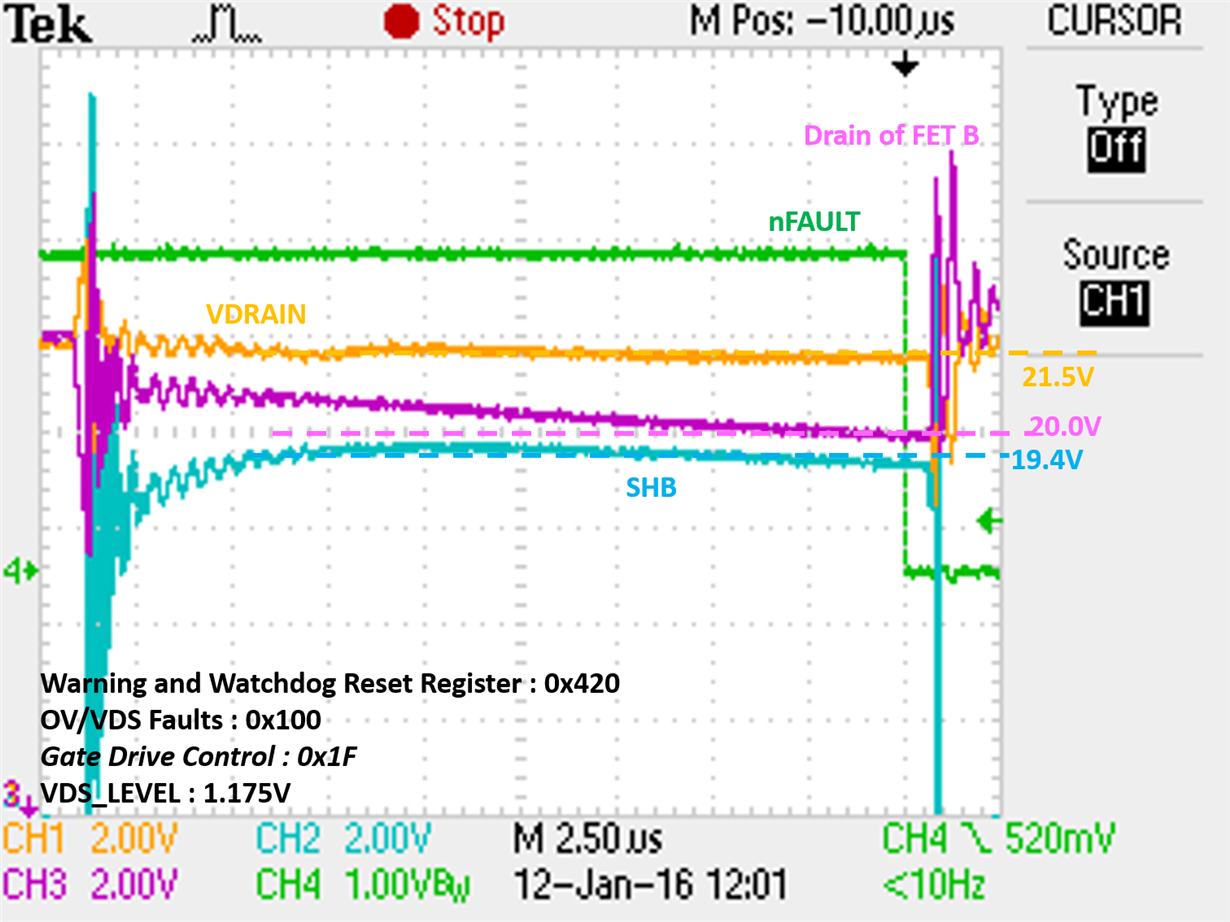
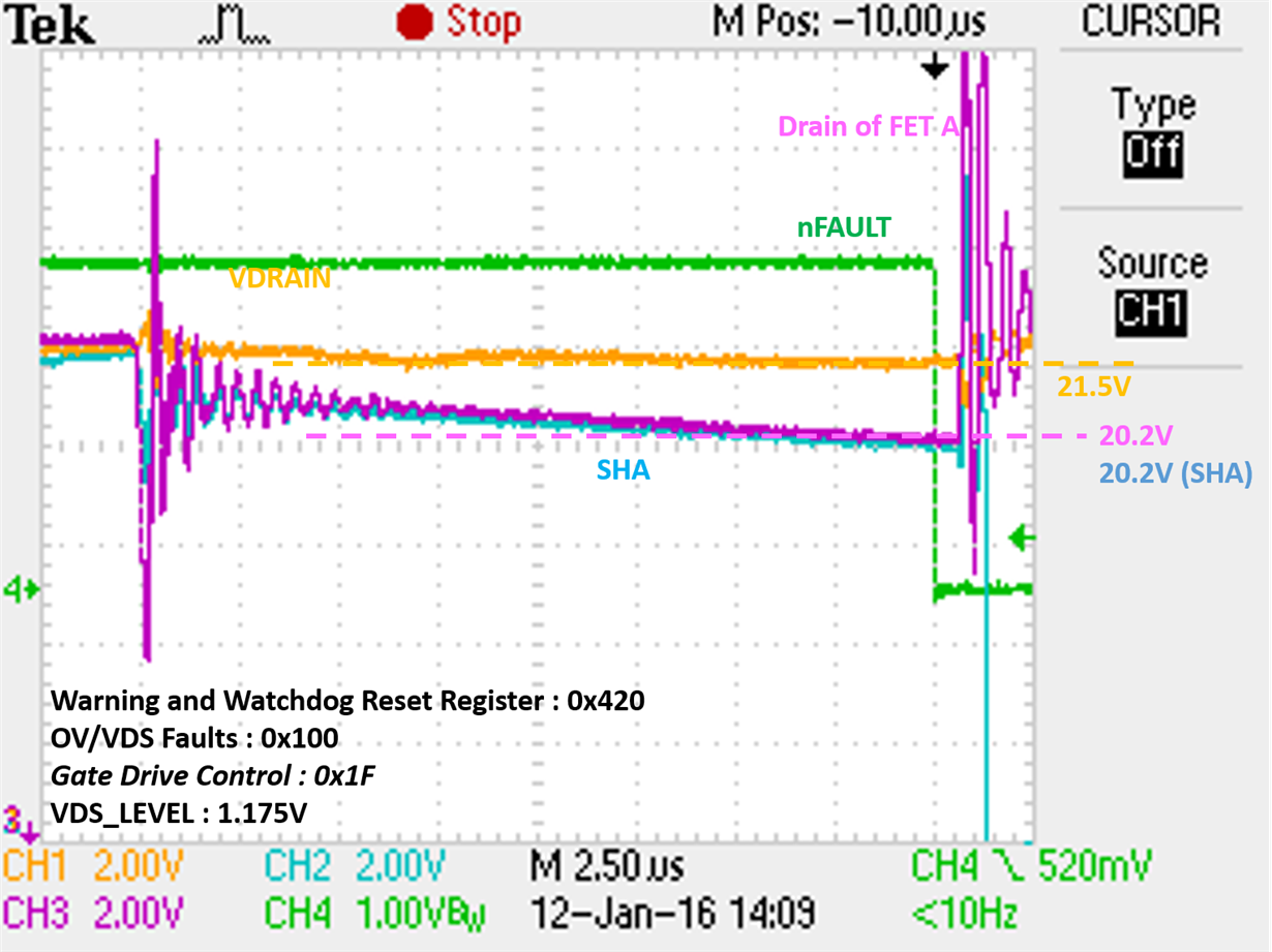
    The following waveforms are cpatured with VDRAIN and FET drain
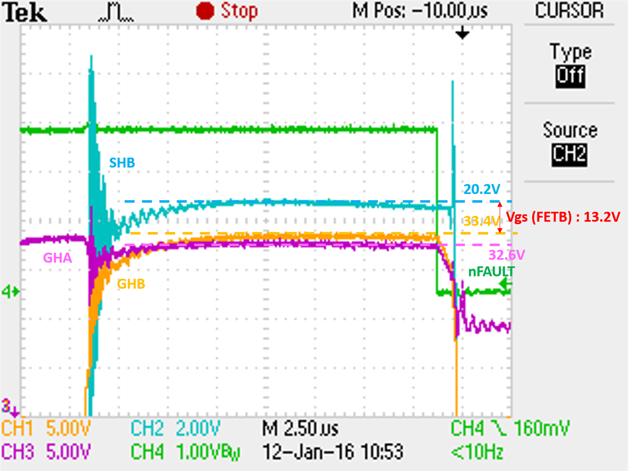
    First one is with VDRAIN and high side FET B drain and source.
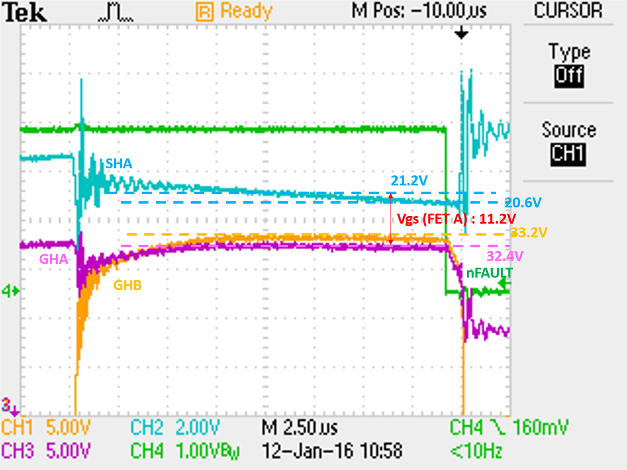
    Second one is with VDRAIN and high side FET A drain and source.
    Drains of FET A and FET B are dropped. (Is this problem??)
    source of FET A has almost same voltage as drain of FET A, but source of FET B voltage is less than drain of FET B and so the voltage between VDRAIN and FET B is large.

    In order to know why source of FET B voltage is less than source of FET A, Vgs of FET A and FET B are measured.
    The waveform which shows Vgs is below.
    Vgs of FET B is higher than Vgs of FET A and so Vgs may not the reason why source of FET B voltage is less than source of FET A.
    Do you have any idea?
    Is there any signal to be captured in order to solove the problem?

  • Hi Shirai-san,

    Thank you for the scope captures. It appears the PVDD connected to the FETs droops more than PVDD connected to VDRAIN. This may be creating false VDS faults.

    How is the connection from VDRAIN to PVDD made on the board? Ideally, the PVDD from FETB should be routed through the 100 Ohm resistor to VDRAIN. This will provide an accurate VDS.

    If possible, please try to edit the board by adding a wire from the PVDD bus near the high sides FETs to the VDRAIN pin. Then try the VDRAIN to SHx (VDS) measurements again.
  • Hi Rick-san,

    Thank you for your reply.

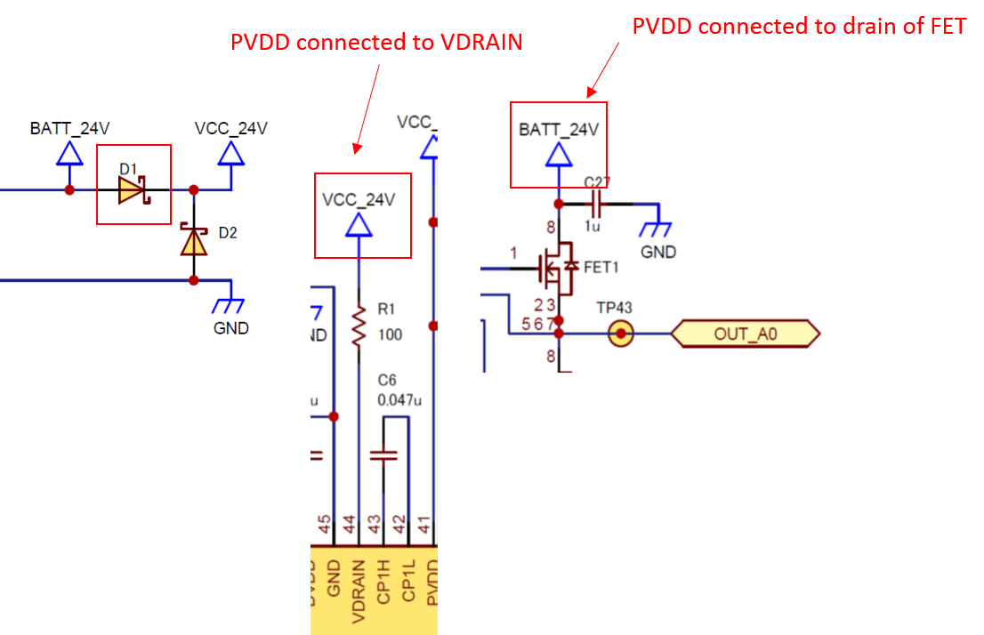
    I found a diode between PVDD connected to VDRAIN and PVDD connected to drain of FET in our board.

    See the schematics below.

    The diode causes the problem.
    Becasue of the diode, PVDD connected to drain of FET is lower than PVDD connected to VDRAIN.
    Accroding to your advise, I tried to add a wire PVDD connected to drain of FET to the VDRAIN pin with 100 Ohm and then the problem was sloved (VDS fault didn't occur!).
    Thank you for your help!!

    Finally, I have quetions about VDRAIN and PVDD
    1.
    Must PVDD connected to VDRAIN with 100 Ohm be the same voltage of PVDD pin of DRV8305?
    I'll connect BATT_24V to VDRAIN with 100 Ohm but wonder if connecting BATT_24V to PVDD pin of DRV8305 or VCC_24V to PVDD pin of DRV8305 because BATT_24V is oscillating with motor load but VCC_24V isn't.
    So is it better to connect VCC_24V to PVDD pin of DRV8305??

    2.
    At Figure 17. Layout Recommendation in datasheet of DRV8305, 10kOhm is used between PVDD and VDRAIN. Is it typo, right?
    The datasheet revision is SLVSCX2A –AUGUST 2015–REVISED SEPTEMBER 2015.

    Best regards,
    Shirai

  • Hi Shirai,

    1. PVDD and VDRAIN do not need to be at the same voltage. The spec currently allows +/- 10V. We use the 100 ohms to limit current into the VDRAIN pin. It is OK to use either VCC_24V or BATT_24V for PVDD. VDRAIN should connect to BATT_24V through the 100 Ohm. One thing to note is that the high-side gate voltage (VCPH) is derived with respect to PVDD, not VDRAIN. So GH_X will be PVDD + 10V approximately, thus the +/-10 V spec for standard MOSFET gate to source ratings of 20V.

    2. Yes, this is a typo.

  • Hi, Nick-san,

    Thank you for your answer.
    I understood well.

    Best,
    Shirai