This thread has been locked.

If you have a related question, please click the "Ask a related question" button in the top right corner. The newly created question will be automatically linked to this question.

DRV8432 datasheet package pin numbering

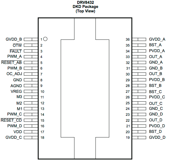
I just looked at the pin numbering on the DRV8432 and it is confusing as hell. In the top you have:

Then on the first package part page you have:

So according to those, you have the cutted edge with pin 1, but pin 36 is no longer opposite of pin 1.

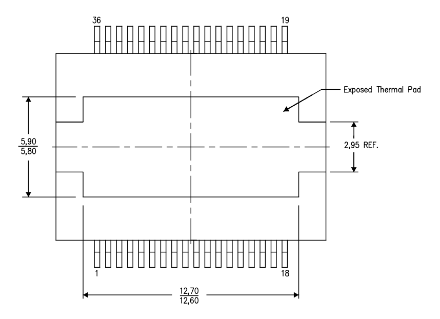
This is the last package one where the pins are like in the first diagram. And then finally, there is reality....

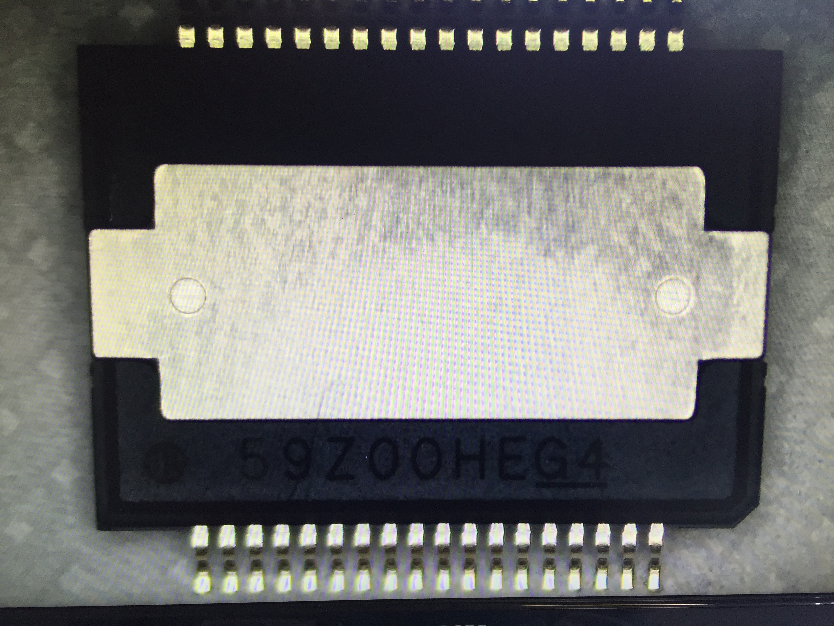
Where the pin 1 marker dot is not on the same edge as the cutted edge.....

Please tell me where pin 1 and where pin 36 is...

  • Hi Karsten,

    Please refer to post e2e.ti.com/.../829466 for a prior discussion.

    Pin 1 location is designated by the circle with 3 lines. The package is used for both a pad up and pad down configurations. This causes the notched corner to be in the wrong position for the DRV8432.

    The mechanical drawing incorrectly identifies pin 19 across from pin 1. Please ignore the numbering on the mechanical drawing. All other drawings appear to be correct.

    A final check is the .bxl file available for the DRV8432 under the www.ti.com/.../quality folder. The .bxl file is a generic schematic symbol and layout footprint portable to many layout tools.